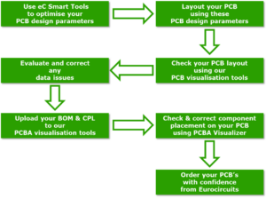
PCB design starts at the conceptual stage, with early consideration of these factors through schematic capture and finally PCB design. Starting later in the design cycle usually involves more complex and expensive designs (the cost of which will grow exponentially over time), sometimes even delaying the board’s lead time. Even with complex and expensive filtering and shielding methods, poor pcb designs or system-level PCB designs are often not corrected. With early intervention and consideration, much of the trouble and expense can be avoided. Design for EMC and SI should include the following major steps:
§Advanced architecture and system planning
§Define applicable standards and requirements
§ Schematic capture and definition of critical networks
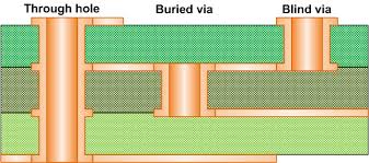
§Select PCB stack to provide design guidelines and constraints for PCB layout
§Component placement-review
§Decoupling, bypass, I / O and critical routing-review
§Non-critical routing-review
§Power and ground plane – review
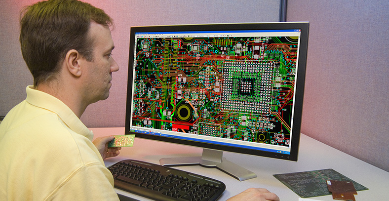
We can bring our expertise in high-speed PCB design to our customers. We can provide review of specifications and schematics and work with customers to generate detailed input information to transition from electrical design (schematics) to physical design (PCB layout, chassis/system considerations). We can also provide guidance and assistance in troubleshooting and act as a liaison for obtaining EMC testing, reports and certificates.

