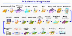
This section will be the final chapter in our introduction to the PCB manufacturing process.
Step 7: Drilling
Finally, drill the holes in the stacked plate. All components planned for later, such as copper connections on the through-hole and lead side, rely on precision drilling for accuracy. The holes are drilled to the same width as a hair-the drill bit reaches 100 microns in diameter, while the average diameter of a hair is 150 microns.
To find the location of the drill target, the X-ray locator identifies the appropriate drill target point. Then, holes are punched in the appropriate locating holes to fix the stack used for a series of more specific holes.
Before drilling, the technician places a piece of cushioning material under the drill target to ensure clean drilling. The exit material prevents any unwanted tearing of the drill exit.
A computer controls every tiny movement of the drill – the product that determines the machine’s performance naturally relies on the computer. This computer-driven machine uses the drill file from the original design to identify the proper drill position.
The drill uses a pneumatic spindle with a speed of 150,000 rpm. At this speed, you might think that drilling is instantaneous, but there are a lot of holes to drill. An average PCB contains over a hundred complete points. Each drill bit requires its own special moment during the drilling process and therefore takes time. The holes will then accommodate the PCB’s over-hole and mechanical mounting holes. The final fixing of these parts takes place after plating.
After drilling is complete, the additional copper lining the edges of the production panel is removed with the profiling tool.
Step 8: Plating and Copper Deposition
After drilling, the panel is moved to the plating layer. The process uses chemical deposition to fuse the different layers together. After a thorough cleaning, the panels are subjected to a series of chemical baths. In a molten bath, the chemical deposition process deposits a thin layer of copper (about one micron thick) on the panel surface. The copper enters the recently drilled holes.
Before this step, the inner surface of the hole exposes only the fiberglass material that forms the interior of the panel. The copper groove completely covers or covers the walls of the hole. Incidentally, the entire panel receives the new copper layer. Most importantly, the new holes are covered. The computer controls the entire process of impregnation, removal and processing.
Step 9: Develop
In step 3, we applied the photoresist to the panel. In this step, we will do it again – except this time, we use the PCB design to develop the outer layer of the panel. We first place the layers in a sterile room to prevent any contaminants from adhering to the layer surface, and then apply a layer of photoresist to the panel. The prepared panels go into the yellow room. UV light affects the photoresist. The UV levels at yellow wavelengths are not sufficient to affect the photoresist.
Black ink transparencies are held in place by pins to prevent alignment with the panel. When the panel and stencil come into contact, the generator sandblasts it with high-intensity UV light, which hardens the photoresist. The panel then enters the machine, which removes the unhardened resist and is protected by the black ink opacity.
This process is the reverse of the process for the inner layer. Finally, the outer plate is checked to ensure that all unwanted photoresist was removed in the previous stage.
Step 10: Plating
We go back to the plating chamber. As we did in step 8, we plated a thin layer of copper on the panel. The exposed portion of the panel from the outer photoresist table receives the plated copper. After the initial copper plating bath, the panel typically receives a tin plating, which removes all of the copper that is scheduled to be removed from the panel. The tin protects a portion of the panel to remain covered with copper during the next etch stage. Etching removes the unwanted copper foil from the panel.
Step 11: Final etching
At this stage, tin protects the desired copper. Remove unwanted bare copper and residual copper below the resist layer. Again, a chemical solution is applied to remove the excess copper. At the same time, tin protects valuable copper at this stage.
Conductive regions and connections have now been properly established.
Step 12: Solder Resist Film Application
Before applying the solder resist to both sides of the board, the panel is cleaned and covered with epoxy solder resist ink. The board receives a beam of UV light that passes through the solder resist photographic film. The covered portion remains unhardened and will be removed.
Finally, the board goes into the oven to cure the solder resist.
Step 13: Surface preparation
To increase the solderability of the PCBs, we chemically plated them with gold or silver. Some PCBs also receive hot air pads during this stage. Hot air leveling produces a uniform pad. This process results in the production of a surface finish. PCBCart can handle many types of surface finishes depending on the specific requirements of the customer.
Step 14: Silkscreening
The soon-to-be-finished board receives inkjet writing on its surface, which is used to indicate all important information related to the PCB. The PCB finally enters the final coating and curing phase.
Step 15: Electrical testing
As a final precaution, the technician performs electrical testing on the PCB. The automated procedure confirms the functionality of the PCB and its conformance to the original design. At PCBCart, we offer advanced electrical testing called “flying probe testing”, which relies on moving probes to test the electrical performance of each network on a bare board.
Step 16: Profiling and V-grooves
Now we come to the final step: cutting. Cutting out different panels from the original panel. The methods used either focus on using a router or on using a v-slot. The router planer leaves small protrusions along the edge of the board, while the v-slot cuts diagonal channels along the sides of the board. Both methods allow the board to be easily ejected from the panel.
