I. PCB surface treatment
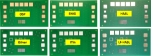
Antioxidation, tin spray, lead-free tin spray, sink gold, sink tin, sink silver, hard gold plating, full board gold plating, gold finger, nickel palladium gold OSP: lower cost, good solderability, harsh storage conditions, short time, environmentally friendly process, good solder, flat.
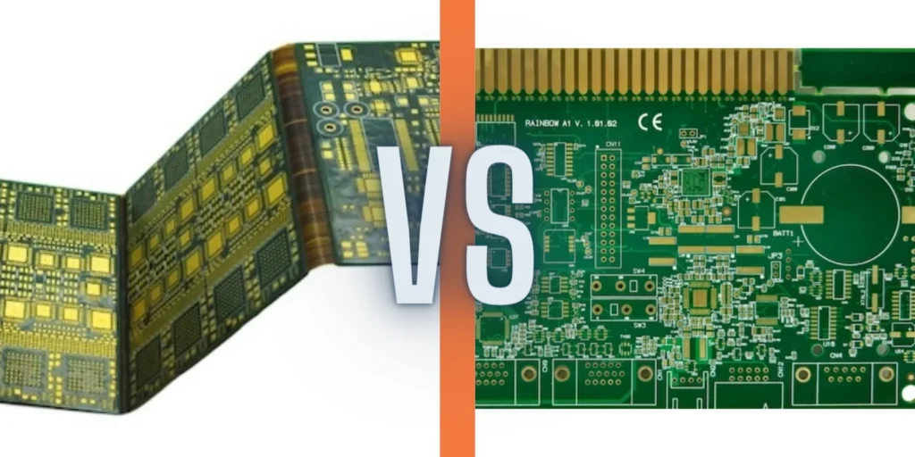
Spray tin: Spray tin boards are generally multi-layer (4-46 layers) high precision PCB prototypes that have been used by many large domestic communication, computer, medical equipment and aerospace companies and research units can use the gold finger (connecting finger) is the connecting part between the memory stick on and the memory slot, all signals are transmitted through the gold finger.
Golden Knuckle is made up of a number of gold colored conductive contacts, which are called “Gold Knuckle” due to its gold plated surface and the finger-like arrangement of the conductive contacts. Gold switches are actually a layer of gold overlay on a copper-clad board through a special process, as gold is extremely resistant to oxidation and has a high conductivity. However, because of the expensive price of gold, more memory are currently used instead of tin plating, from the 1990s tin material began to popularize, the current motherboard, memory and graphics cards and other equipment “gold finger” is almost all used in the tin material, only some high-performance server / workstation accessories contact points will continue to use gold-plated The price is naturally not expensive.
II. Why gold-plated boards
As ICs become more and more integrated, the IC pins become more and more dense. The vertical spray tin process is difficult to blow the pads into a fine flat, which brings difficulty to the SMT placement; in addition, the pending life (shelf life) of the spray tin board is very short. Gold plated boards solve these problems:
1. For surface mount process, especially for 0603 and 0402 ultra-small surface mount, because the pad flatness is directly related to the quality of solder paste printing process, and plays a decisive influence on the quality of the later reflow soldering, so the whole board gold plating is often seen in the high-density and ultra-small surface mount process.
2. In the prototype stage, influenced by factors such as component procurement, the boards are often not soldered immediately, but often have to wait for weeks or even months before they are used, and the life expectancy of gold-plated boards (shelf life) is many times longer than that of lead-tin alloy, so everyone is happy to use them. The cost of gold-plated PCBs is comparable to that of lead-tin alloy boards at the prototyping stage.
But as the wiring has gotten denser, the line widths and spacing have gone to 3-4 MIL.
This brings up the issue of shorted gold wires: as the frequency of the signal gets higher, the more pronounced the impact on signal quality is due to the skin effect causing the signal to be transmitted in multiple plating layers.
The skinning effect is that with high frequency alternating current, the current will tend to flow concentrated on the surface of the wire. The skinning depth is calculated to be frequency dependent.
Three, why sunken gold plates
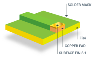
To solve the above problems of gold-plated boards, PCBs with gold-sink boards have the following main features:
1. Because of the different crystal structures formed by submerged gold and gold plating, submerged gold will be more yellow in color than gold plating, making customers more satisfied.
2. Because of the different crystal structures formed by submerged gold and gold plating, submerged gold is easier to solder than gold plating and will not cause poor soldering and customer complaints.
3. Because only the pads on the sinker board have nickel-gold, the transmission of signals in the skin effect is in the copper layer will not affect the signal.
4. Because of the denser crystal structure of sunken gold compared to gold plating, it is less likely to cause oxidation.
5. Because the sinker plate only has nickel-gold on the pads, it does not produce gold wire resulting in a micro-short.
6. Because only the pads on a sinker board have nickel-gold, the solder resist on the line is more firmly bonded to the copper layer.
7. The project does not affect the spacing when making compensation.
8. Because the crystal structure formed by sinker gold and gold plating is different, the stress of its sinker gold plate is easier to control, which is more conducive to the processing of bonding for products with bonding. Also because sink gold is softer than gold plating, so sink gold plates do not wear out gold fingers.
9. The flatness and life to be used of the sunken gold plate is as good as that of the gold plated plate.
IV. Submerged gold vs. gold plated plates
For the gold plating process, the tin effect is greatly reduced, while the tin effect is better for the submerged gold; unless the manufacturer requires a binding, most manufacturers now choose the submerged gold process! The general common case of PCB surface treatment for the following kinds: gold plating (gold plating, sinking gold), silver plating, OSP, spray tin (lead and lead-free), these are mainly for FR-4 or CEM-3 and other plates, paper-based materials and coated rosin surface treatment; on the tin bad (eat tin bad) this piece if you exclude the paste and other SMD manufacturers production and material process reasons.
There are several reasons for speaking only to the PCB issue here:
1. Whether there is an oil seepage film surface on the PAN bit during PCB printing, which can block the effect of tin on; this can be verified by doing a bleaching tin test.
2. Does the PAN bit on the run bit meet the design requirements, that is, whether the pad design can be sufficient to ensure the support role of the part.
3. The pads have not been contaminated, which can be derived from ionic contamination testing; the above three points are basically the key aspects considered by PCB manufacturers.
The pros and cons of several approaches to surface treatment are each with their own strengths and weaknesses!
In terms of gold plating, it allows the PCB to be stored for a longer period of time and is less subject to external changes in ambient temperature and humidity (compared to other surface treatments), and can generally be stored for about a year; the sprayed tin surface treatment follows, and OSP follows, and both surface treatments require much more attention in terms of ambient temperature and humidity storage time.
In general, sinker silver has a somewhat different surface treatment, is more expensive, and has more demanding preservation conditions, requiring a sulfur-free paper packaging treatment! And the preservation time is around three months! In terms of tin effect, sink gold, OSP, spray tin, etc. are actually about the same, and manufacturers are mainly considering the cost effectiveness aspect!

