I. PCB concept
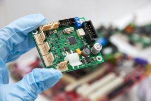
PCB (Printed Circuit Board), the Chinese name for printed circuit board, also known as printed circuit board, printed circuit board, is an important electronic component, a support body for electronic components, and a provider of electrical connections for electronic components. It is also known as a “Printed” circuit board, as it is made using electronic printing techniques.
II. The role and function of PCBs in various electronic devices
1. Pad: Provides mechanical support for fixing and assembling various electronic components such as integrated circuits.
2. Alignment: Enables wiring and electrical connections (signal transmission) or electrical insulation between various electronic components such as integrated circuits. Provides the required electrical characteristics, such as characteristic impedance.
3. Green oil and silkscreen: provide solder resist graphics for automatic assembly, and identification characters and graphics for component insertion, inspection, and repair.
III. Summary of PCB technology development from 1903 to present, if we look at the application and development of PCB assembly technology, it can be divided into three stages
1. Through-Hole-Thru-Technology (THT) stage PCB
1. Role of metalized holes:
(1). Electrical interconnection — signal transmission
(2). Support components — pin size limits through-hole size reduction
a. Rigidity of pins
b. Requirements for automated insertion
2. Ways to increase density
(1) Reduce the size of the device hole, but limited by the rigidity of the component pins and the accuracy of insertion, with a hole diameter ≥ 0.8 mm
(2) Reduced line width/spacing: 0.3mm-0.2mm-0.15mm-0.1mm
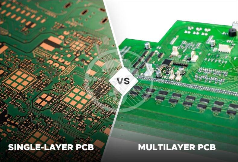
(3) Adding layers: single-sided – double-sided – 4 layers – 6 layers – 8 layers – 10 layers – 12 layers – 64 layers
3. Surface mount technology (SMT) stage PCB
(1). The role of the pilot hole: it only serves as an electrical interconnection, the hole can be as small as possible, and plugging the hole is fine.
(2). Key ways to increase density
①. Dramatic reduction in over-hole size: 0.8mm-0.5mm-0.4mm-0.3mm-0.25mm
②. The structure of the perforations has changed in nature:
a. Advantages of buried blind vias: increased wiring density by more than 1/3, reduced PCB size or layer count, increased reliability, improved characteristic impedance control, reduced crosstalk, noise or distortion (due to short lines and small vias)
b. Hole in pad eliminates relay holes and linkages
(3) Thinner: dual panel: 1.6mm-1.0mm-0.8mm-0.5mm
(4) PCB flatness:
a. Concept: PCB board substrate warpage and the coplanarity of the surface of the connection plate on the PCB board surface.
b. PCB warpage is the result of a combination of thermal and mechanical induced residual stresses
c. Surface coating of connection plates: HASL, chemically plated NI/AU, electroplated NI/AU…
4. Chip-level packaging (CSP) stage PCB
CSP is starting to enter a dramatic change in development, driving PCB technology forward and moving the PCB industry towards the laser and nano era.
IV. PCB surface coating technologyPCB surface coating technology refers to the solderable coating (plating) layer and protective layer for pneumatic connections other than solder resist coating (and protection) layer.
By use:
1. For soldering: Because the surface of copper must be protected by a coating layer, otherwise it will easily oxidize in the air.
2. For connectors: Electroplated Ni/Au or chemically plated Ni/Au (hard gold with P and Co)
3. For wire bonding: wire bonding process
Hot air leveling (HASL or HAL)
PCBs coming out of molten Sn/Pb solder are blown flat by hot air (230°C).
1. Basic requirements:
(1). Sn/Pb=63/37 (weight ratio)
(2). Coating thickness of at least >3um
(3) Avoid the formation of non-solderable Cu3Sn, which occurs when the amount of tin is insufficient, e.g., the Sn/Pb alloy coating layer is too thin and the solder joint composition consists of solderable Cu6Sn5 – Cu4Sn3 – Cu3Sn2 – non-solderable Cu3Sn
2. Process flow
Resist removal – Board cleaning treatment – Solder resist and character printing – Cleaning treatment – Flux application – Hot air leveling – Cleaning treatment
3. Disadvantages:
a. The lead-tin surface tension is too high, which is easy to form turtle back phenomenon. b. The pad surface is not flat, which is not good for SMT soldering. Chemically plated Ni/Au means the PCB connection plate is chemically plated with Ni (thickness ≥3um) followed by a thin layer of 0.05-0.15um gold, or a thick layer of gold (0.3-0.5um). Because of the chemical plating uniform, coplanar good, and can provide multiple welding performance, therefore has the trend of promoting the application. Which plating thin gold (0.05-0.1um) is to protect the Ni solderability, and plating thick gold (0.3-0.5um) is for wire bonding (wire bonding) process needs.
1. What the Ni layer does:
a. Acts as an isolation layer between Au and Cu to prevent them from spreading to each other, causing their spreading sites to be sparse.
b. As a solderable plating with a thickness of at least >3um
2. Au is the protective layer of Ni, thickness between 0.05-0.15, can not be too thin, because the gold is more porous if too thin can not be well protected Ni, causing Ni oxidation. Its thickness can not > 0.15um, because the solder joint will form a gold-copper alloy Au3Au2 (brittle ), when the Au in the solder joint more than 3%, the weldability becomes poor.
3. Plating Ni/Au
The plating structure is basically the same as chemical Ni/Au, the uniformity of the plating is less due to the plating method.
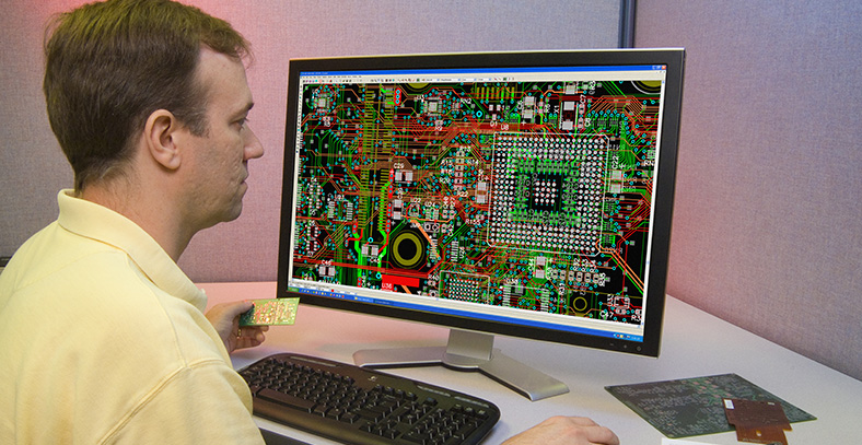
V. PCB design output production files Caution
1. The layers that need to be output are: (1). Wiring layers including top/bottom/intermediate wiring layers;
(2). The silkscreen layer includes the top silkscreen/bottom silkscreen;
(3). The solder resist layer consists of a top layer resist and a bottom layer resist;
(4). The power layer includes the VCC layer and the GND layer;
(5). Also generate the drill file NCDrill.
2. If the power layer is set to Split/Mixed, then select Routing in the Document item of the AddDocument window and use PourManager’s Plane Connect to overlay the PCB before each output of the light painting file; if it is set to CAMPlane, then select Plane and add Layer25 to Layer25 and select Pads and Vias in Layer25 when setting the Layer item.
3. Press Device Setup in the Device Setup window to change the value of Aperture to 199.
4. Leave BoardOutline checked when setting up Layers for each layer.
5. Do not select PartType when setting the Layer for the silkscreen layer Select the top bottom layer and the Outline Text Line for the silkscreen layer.
6. Selecting Over Hole when setting the Layer for the solder resist layer means that no solder resist is added to the over hole. Usually overholes are covered by a solder resist layer.
Sixth, safety marking requirements 1. The safety marking of the fuse is complete whether there are 6 complete markings near the fuse, including fuse serial number, fusing characteristics, rated current value, explosion-proof characteristics, rated voltage value, and English warning markings. Such as F101 F3.15AH,250Vac, “CAUTION: For ContinuedProtection Against Risk of Fire, Replace Only With SameType and Rating of Fuse” . If there is no space on the PCB to line up the English warning label, you can put the work, English warning label into the product’s instruction manual to explain.
2. The hazardous voltage area on the PCB is marked with a high voltage warning symbol The hazardous voltage area portion of the PCB should be isolated from the safe voltage area with a 40 mil wide dotted line and printed with the high voltage hazard symbol and ” DANGER!
3. The original and paid edge separation zone is clearly marked The original and paid edge separation zone of the PCB is clearly marked with a dotted line in the middle.
4. PCB board safety markings should be clear and complete.
VII.PCB EMI DesignThe most common problem in PCB design is the signal lines crossing the split ground or power supply and creating EMI problems. To circumvent this EMI problem here is a step-by-step guide to EMI design specifications for PCB design.
1. Power handling of ICs
Ensure that each IC’s power PIN has a 0.1μF decoupling capacitor. For BGA CHIP, a total of 8 capacitors of 0.1μF and 0.01μF are required at the four corners of the BGA respectively. Particular attention should be paid to the power supply of the alignment to add filtering capacitors, such as VTT, etc. This not only has an impact on stability, but also has a great impact on EMI. General decoupling capacitors still need to follow the requirements of the chip manufacturer.
2. Handling of clock lines
1. It is recommended that the clock line be taken first.
2. For clock lines with frequencies greater than or equal to 66M, the number of vias should not exceed 2 per line, and the average should not exceed 1.5.
3. For clock lines with frequencies less than 66M, the number of vias per line should not exceed 3, and the average should not exceed 2.5
4. For clock lines longer than 12inch, if the frequency is greater than 20M, the number of vias must not exceed 2.
5. If the clock line has a vias, add a bypass capacitor between the second (ground) and third (power) layers, as shown in Figure 2.5-1, adjacent to the vias, to ensure a continuous loop of high frequency current in the reference layer (adjacent layer) after the clock line changes layers. The power layer where the bypass capacitor is located must be the power layer through which the vias pass, and as close to the vias as possible, with the bypass capacitor spacing from the vias not exceeding 300 MIL maximum.
6. All clock lines are in principle not to be islanded (across the division). The four cases of island crossing are listed below.
Clock, reset, 100M+ signals, and some critical bus signals cannot span a split and have at least one full plane, preferably the GND plane.
Clock signals, high-speed signals and sensitive signals are prohibited across the segmentation;
Differential signals must be balanced to ground to avoid single line across the split. (Try to cross split vertically)

The high-frequency return paths for all signals are located directly below the signal lines of the adjacent layers. Signal integrity and timing issues can be significantly reduced by having a solid layer below the signal that provides a direct loop for that signal. A 0.01 uF loop capacitor should be used when crossover of the alignment and layer split is unavoidable. When using a loop capacitor, the loop capacitor should be placed as close as possible to the intersection of the signal line with the layer split, as shown in the figure.
6.1 The cross-island appears between the power island and the power island. In this case, the clock line is routed on the back of the fourth layer, the third layer (power layer) has two power islands, and the fourth layer must be routed across both islands.
6.2 The cross-island appears between the power island and the ground island. In this case, the clock line is routed on the back of layer 4, there is a ground island in the middle of one of the power islands on layer 3 (the power layer), and the layer 4 alignment must span both islands.
6.3 The cross-island appears between the ground island and the ground layer. In this case, the clock line is aligned on the first level, there is a ground island in the middle of the second level (ground level), and the alignment on the first level must cross the island, which is equivalent to the ground line being interrupted.
6.4 No copper is laid under the clock line. If the conditions are too restrictive to do without islanding, ensure that the clock line with a frequency greater than or equal to 66M is not islanded, and if the clock line with a frequency less than 66M is islanded, a decoupling capacitor must be added to form a mirror path. In Figure 6.1, for example, between the two power islands and near the cross-island clock line, place a capacitor of 0.1UF.
7. When faced with the trade-off between two overholes and one island piercing, choose one island piercing.
8. The clock line should be more than 500MIL away from the I/O side of the board, and do not walk alongside the I/O line, if this is not possible, the clock line and the I/O port line spacing should be greater than 50MIL.
9. When the clock line goes in the fourth layer, the reference layer (power plane) of the clock line should try to power the clock on that power plane, the less the clock is referenced to other power planes, the better. In addition, the reference power plane of the clock line with a frequency greater than or equal to 66M must be the 3.3V power plane.
10. Clock lines should be spaced more than 25MIL apart when typing the lines.
11. The line going in and the line going out should be as far apart as possible when the clock line is punched. Try to avoid typing like the one shown in Figure A and Figure C. If the clock line needs to change layers, avoid the typing in Figure E and use the typing in Figure F.
12. When connecting clock lines to BGAs and other devices, if the clock lines change layers, try to avoid using the alignment form in Figure G. The vias should not go underneath the BGA, but preferably use the alignment form in Figure H.
13. Pay attention to each clock signal, do not ignore any of the clocks, including AUDIO CODEC’s AC_BITCLK, pay particular attention to FS3-FS0, although the name does not look like a clock, but actually running a clock, pay attention to it.
14. Clock Chip pull-up pull-down resistors as close to the Clock Chip as possible.
3. Handling of I/O ports
1. Each I/O port including PS/2, USB, LPT, COM, SPEAK OUT, GAME is divided into one piece of ground, the leftmost and rightmost are connected to the digital ground, the width is not less than 200MIL or three overholes, and the other places are not connected to the digital ground.
2. If the COM2 port is plugged in, place it as close to the I/O ground as possible.
3. I/O circuit EMI devices as close to the I/O SHIELD as possible.
4. Separate islands for the power and ground layers at the I/O ports, and both the Bottom and TOP layers should be grounded, with no signals allowed through the islands (signal lines are pulled directly out of the PORT, not in the I/O PORT for long distances).
4. A few notes
1. The EMI design specification should be strictly adhered to by the design engineer, and the EMI engineer has the right to check it. The responsibility of violating the EMI design specification and leading to EMI test FAIL is borne by the design engineer.
2. EMI engineers are responsible for design specifications, for strict compliance with EMI design specifications, but still EMI testing FAIL, EMI engineers have the responsibility to give solutions and summarize them into EMI design specifications.
3. EMI engineers are responsible for the EMI testing of each peripheral port and must not miss testing.
4. Each PCB design engineer has the right to suggest changes to the design specification and the right to challenge it. it is the responsibility of the EMI engineer to answer the challenge and to add the engineer’s suggestion to the design specification after it has been confirmed by experimentation.
5. It is the responsibility of the EMI engineer to reduce the cost of the EMI design and to reduce the number of beads used.
