Eight, ESD suppression for PCB design
PCB routing is a critical element of ESD protection, and proper PCB design can reduce unnecessary costs associated with failure checking and rework. With the use of transient voltage suppressor (TVS) diodes to suppress direct charge injection due to ESD discharge, PCB design is more important to overcome electromagnetic interference (EMI) electromagnetic field effects generated by the discharge current. This article will provide PCB design guidelines that can optimize ESD protection.
1. Circuit loops
Current enters through induction into circuit loops that are closed and have a varying flux. The amplitude of the current is proportional to the area of the loop. Larger loops contain more flux and thus induce stronger currents in the circuit. Therefore, the loop area must be reduced.
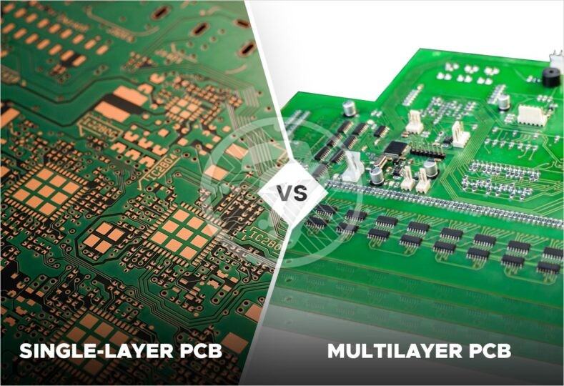
The most common loops are formed by power and ground. Whenever possible, a multilayer PCB design with power and ground layers can be used. Not only does a multilayer PCB minimize the loop area between power and ground, but it also reduces the high frequency EMI fields generated by ESD pulses.
If a multilayer board is not possible, then the wires for power and ground must be connected in a grid pattern. The grid connection serves as a power and grounding layer. The printed wires on each layer are connected with vias, and the vias should be spaced within 6 cm of each other in each direction. In addition, wiring the power and ground printed wires as close together as possible can also reduce loop area.
Another way to reduce loop area and induced current is to reduce the parallel path between interconnect devices.
When a signal connection line longer than 30 cm must be used, a protective line can be used. A better approach is to place a ground layer near the signal line. The signal line should be within 13 mm of the protective or ground layer.
Cross each sensitive element’s long signal wire (>30 cm) or power wire with its ground wire. The crossed wires must be laid out at regular intervals from top to bottom or left to right.
2. Circuit connection length
Long signal lines can also be antennas for receiving ESD pulse energy. Using shorter signal lines as much as possible can reduce the efficiency of the signal lines as antennas for receiving ESD electromagnetic fields.
Try to place the interconnected devices as close together as possible to reduce the length of the interconnected printed lines.
3. Ground charge injection
The direct discharge of ESD to the ground layer can damage sensitive circuits. One or more high-frequency bypass capacitors are used in conjunction with TVS diodes, which are placed between the power and ground of the vulnerable components. The bypass capacitor reduces charge injection and maintains the voltage difference between the power supply and the ground port.
The TVS shunts the induced current and maintains the potential difference of the TVS clamp voltage. the TVS and capacitor should be placed as close as possible to the IC being protected, making sure the TVS to ground path and the capacitor pin length are the shortest possible to reduce parasitic inductance effects.
IX. Mark point design in PCB production
1. pcb must have a Mark point on the diagonal of the long side of the board corresponding to the positioning of the whole board, the chip on the board IC pin center distance less than 0.65mm need to have a pair of Mark points on the diagonal of the long side of the IC corresponding to the positioning of the chip; pcb both sides have SMD parts, then both sides of the pcb add Mark points according to this article.
2. pcb edge need to leave 5mm process edge (machine clamping pcb minimum spacing requirements), at the same time should ensure that the integrated circuit pin center distance less than 0.65mm chip to be greater than 13mm from the edge of the board (including process edge); board corners with Ф5 rounded chamfer. pcb should be used to put together the board, from the current pcb fin curved degree of consideration, the best splicing length of about 200mm, (equipment processing Size: length up to 330mm; width up to 250mm), in the width direction as far as possible not to spell to prevent bending in the production process. The figure below:
3. MARK point roles and categories
Mark points, also called datum points, provide a common measurable point for all steps in the assembly process, ensuring that each device used in the assembly can accurately position the circuit pattern. Therefore, Mark points are critical to SMT production
4. Our department’s recommended MARK point design specifications
1) Shape: The recommended Mark point marker is a solid circle with diameter: R=1.0mm;
2) The points that make up a complete MARK include: marker points (or feature points) and empty areas.
3) Location: Mark points are located diagonally opposite each other and as far apart as possible on the veneer or plywood; preferably distributed in the longest diagonal positions (as in the MARK point location diagram).
4) In order to ensure the requirements of placement accuracy, SMT requires that: there must be at least one pair of MARK points within each PCB that can be recognized by SMT machines in accordance with the design requirements, and there must be a single board MARK (when assembling boards), and the assembled board MARK or combined MARK only plays the role of auxiliary positioning.
5) The relative positions of the MARK points on each veneer must be the same when putting the board together. You can’t move the position of the MARK points on any of the veneers for any reason, resulting in an asymmetric position of the MARK points on each veneer.
6) All MARK points on a PCB are only valid if they are on the same diagonal and occur in pairs. So MARK points must all be in pairs to be used (MARK point location map).
7) The MARK point (edge of the empty area) must be ≥5.0mm from the edge of the PCB (minimum spacing required for machine clamping of the PCB) (as shown in the MARK point location diagram).
8) dimensions
A. The minimum diameter of the mark dot mark is 1.0mm, the maximum diameter is 3.0mm, and the mark dot mark cannot vary in size by more than 25 microns on the same printed board;
B. Special emphasis: all Mark dots must be the same size on the same board number PCB (including PCBs of the same board number from different manufacturers);
C. It is recommended that all Mark point markers be set to a uniform diameter of 1.0mm.
9) Empty area requirement
A void area free of other circuit features or markers must be present around the Mark point marker. The radius of the empty area circle r≥2R , R is the radius of the MARK point,r reaches 3R for better machine recognition.
10) Materials
Mark dot markers can be bare copper, clear, bare copper protected by an anti-oxidation coating. If soldermask (solder resist) is used, it should not cover the Mark point or its open areas
11) The luminosity of the MARK points should be consistent.
12) Flatness: Mark point markers should have a surface flatness of 15 microns or less.
13) Contrast
A. Best recognition performance is achieved when there is a high contrast between the Mark dot mark and the substrate material of the printed board
B. For all Mark points the inner background must be the same

