There are multiple classification methods for PCB (printed circuit board) circuit boards, and the following is a detailed summary based on different classification standards:
1、 Classified by the number of layers of conductive patterns
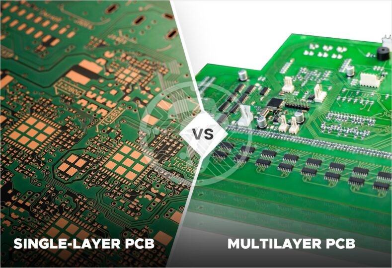
Single panel: The most basic type of PCB, with parts concentrated on one side and wires concentrated on the other side.
Because the wires only appear on one side, it is called a single panel.
Mainly used in early circuits and simple electronic products, such as household appliances, toys, etc.
There are many strict restrictions on the design of single panel circuits, and wiring cannot cross each other and must follow separate paths.
Double sided board: A PCB with conductive patterns printed on both sides of a double-sided copper-clad laminate, with conductive patterns on both sides. Generally, metalized holes are used to connect the conductive patterns on both sides.
This type of PCB can be interlaced by winding the wiring to the other side through metal holes, so it can be used on more complex circuits, such as computer motherboards, communication equipment, etc.
Multilayer board: A PCB with 3 or more layers of conductive patterns, the inner layer is made by stacking and pressing conductive patterns with insulating semi cured sheets, and the outer layer is made of copper foil, which is pressed into a whole.
In order to lead out the printed wires sandwiched between the insulating substrate, the conductive holes on the multi-layer board need to be metalized to connect with the printed wires sandwiched in the insulating substrate.
The production of conductive patterns on multi-layer boards is mainly based on the photosensitive method, with an even number of layers and including the outermost two layers.
Multilayer boards have the characteristics of high density and high performance, and are suitable for complex electronic devices such as smartphones, tablets, etc.
2、 Classified by board material
Rigid board: Made of a rigid substrate that is not easily bent and has a certain degree of toughness, it has bending resistance and can provide certain support for electronic components attached to it.
Rigid substrates include fiberglass cloth substrates, paper substrates, composite substrates, ceramic substrates, metal substrates, thermoplastic substrates, etc.
Rigid PCBs are widely used in industries such as computer and network equipment, communication equipment, industrial control, consumer electronics, and automotive electronics.
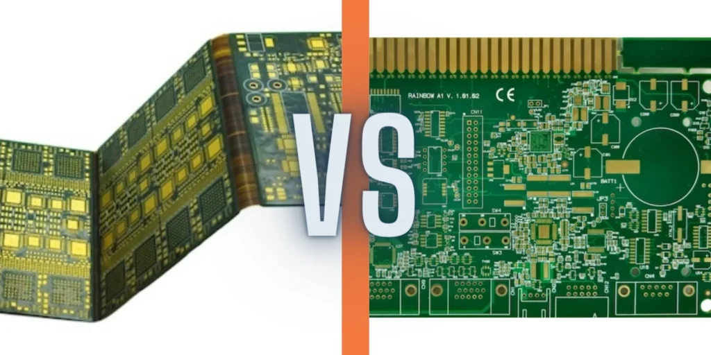
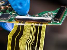
Flexible PCB: also known as FPC, uses flexible materials such as polyimide or polyester film as the substrate.
Flexible boards can be freely bent, wound, and folded, arranged according to spatial layout requirements, and can move and stretch freely in three-dimensional space, thus achieving the integration of component assembly and wire connection.
Widely used in fields such as smartphones, laptops, tablets, and other portable electronic devices.
Rigid flex joint board: It consists of one or more rigid and flexible areas on a PCB, and is formed by laminating a thin layer of flexible printed circuit board bottom layer and a rigid printed circuit board bottom layer.
The rigid flex joint board combines the advantages of rigid PCB and flexible PCB, possessing both the stability and mechanical strength of rigid areas and the bending performance of flexible areas.
It can meet the requirements of 3D assembly and is widely used in advanced medical electronic devices, portable cameras, and foldable computer equipment.
3、 Classified by product structure
Thick copper plate: refers to any PCB with a copper thickness of 3oz or more.
Thick copper plates can carry high currents and voltages, while also having good heat dissipation performance.
Thick copper plates have high requirements for bonding agents, drilling, electroplating, and other processes due to the thick copper thickness of the circuit. They are widely used in industrial power supplies, medical equipment power supplies, military power supplies, engine equipment, etc.
High frequency PCB: also known as high-frequency communication circuit board, RF circuit board, etc., refers to PCB produced using special low dielectric constant and low dielectric loss materials, with high electromagnetic frequency.
High frequency boards have higher requirements for signal integrity and material processing difficulty, which is reflected in stricter requirements for graphic accuracy, interlayer alignment, and impedance control, resulting in higher prices.
Mainly used in communication base stations, microwave communication, satellite communication, radar and other fields.
High speed board: A PCB made of low dielectric loss high-speed materials, mainly responsible for the data transmission, processing, and calculation of high-speed circuit signals between chipsets and between chipsets and peripherals, in order to achieve chip operation and signal processing functions.
High speed boards have high requirements for fine line processing, characteristic impedance control technology, and insertion loss control, and are mainly used in communication and server, storage, switch and other fields.
Metal substrate: a composite PCB composed of a metal substrate, an insulating dielectric layer, and a circuit layer.
Metal substrates have the characteristics of good heat dissipation and excellent mechanical processing performance, and are mainly used in electronic systems with high heat generation, such as LED liquid crystal displays, LED lighting fixtures, car lights, etc.
HDI board: short for High Density Interconnect PCB, also known as micro porous board or laminated board.
HDI boards can achieve high-density wiring and are commonly used to make high-precision circuit boards.
HDI boards are generally manufactured using the layering method, which uses laser drilling technology to drill holes for conduction in the layers, forming interlayer connections with buried and blind holes as the main conduction method for the entire PCB.
Compared to traditional multi-layer PCBs, HDI boards can achieve features such as high-density PCB, fine wire structure, and small aperture size.
Mainly used in high-density demand areas such as consumer electronics, automotive electronics, etc., such as mobile phones, laptops, autonomous driving sensors, etc., among which smartphones are the largest application area of HDI boards.
At present, HDI technology is used in communication products, network products, server products, automotive products, and even aerospace products.
Packaging substrate: Refers to an IC (Integrated Circuit) packaging carrier board, directly used for mounting chips, which can provide electrical connections, protection, support, heat dissipation, assembly and other functions for chips to achieve multi pin design, reduce the volume of packaged products, improve electrical performance and heat dissipation, ultra-high density or multi chip modularization.
4、 Classified by the conductivity status of the holes
Buried hole plate: The holes of this plate are completely buried between the internal conductive layers, and the surface is invisible, suitable for applications that require hidden connections or increased electrical performance.
Blind hole board: The holes of this board are only connected to one surface conductive layer, and the other end is a blind end, commonly used for internal connections in multi-layer boards.
Through hole board: The holes on this board penetrate the entire PCB and connect all conductive layers, making it one of the most common types of PCB.
5、 Classified by surface fabrication
Spray tin plate: Spray a layer of tin on the surface of the conductive layer to protect it and improve soldering performance.
Widely used in processes such as wave soldering and manual soldering.
Gold plating plate: Covering the surface of the conductive layer with a layer of metallic gold to improve conductivity and oxidation resistance.
Suitable for high-end electronic devices such as aerospace, medical equipment, etc.
Sinking gold plate: depositing a gold layer on a copper surface through chemical methods, which has better adhesion and conductivity.
ENTEK board: using special chemical treatment to improve the oxidation resistance and weldability of copper foil.
Carbon oil board: Printing carbon oil lines on insulating substrates for low voltage and signal transmission.
Gold finger board: Expose copper surface at the edge and gold plating, used for connection with other PCBs or modules.
Sinking tin plate: Similar to sinking gold plate, but with the difference of using tin instead of gold deposition, the cost is relatively lower.
