PCB board copying is a complex and intricate process that involves reverse analysis of the original circuit board and restoration of technical files.The following is the entire process of copying PCB circuit boards:
1、 Preparation stage
Obtaining circuit board samples: Firstly, it is necessary to obtain the circuit board samples to be replicated, ensuring that the obtained circuit board samples are intact for subsequent reverse analysis.
Record component information: Record the model, parameters, and position of all components on the circuit board, especially the direction of diodes, transistors, and IC notches.
2、 Dismantling and Cleaning Stage
Dismantling components: Use appropriate tools to disassemble components on the circuit board, taking care to protect the components from damage.
Cleaning the board: Clean the surface of the disassembled circuit board thoroughly, removing any remaining solder and dirt.
3、 Scanning and processing stage
Scanning circuit board: Place the cleaned circuit board into the scanner and obtain a clear image of the circuit board with a higher scanning resolution.
Image processing: Process the scanned circuit board image, adjust the contrast and brightness of the image, then convert the image to black and white mode, and check whether the lines are clear.
4、 File conversion and design phase
File conversion: Convert the processed black and white BMP format circuit board image into a format file that can be recognized by PCB design software.
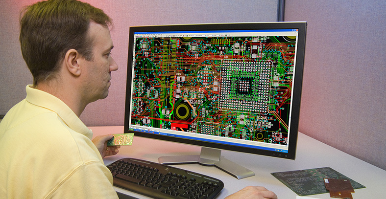
Design circuit board: Import the converted file into PCB design software and start designing the circuit board.
Design the layout, wiring, and component selection of the circuit board based on the extracted and processed data.
5、 Production and welding stage
Produce circuit board: Based on the designed circuit board diagram, use laser cutting, mechanical drilling, and other methods to produce the actual circuit board.
Welding components: Weld the required components onto the circuit board according to the design requirements and positions.
During the welding process, attention should be paid to the welding quality and welding sequence to avoid problems such as virtual welding and short circuits.
6、 Testing and debugging phase
Test circuit board: Test the completed circuit board to check if its functionality and performance meet the requirements.
Debugging circuit board: If any problems or malfunctions are found on the circuit board, debugging and repair are required.
Based on the test results and problem analysis, take appropriate measures to repair and improve.
The entire process of copying PCB circuit boards includes preparation stage, disassembly and cleaning stage, scanning and processing stage, file conversion and design stage, production and soldering stage, testing and debugging stage, and merging and verification stage (optional).
Each stage has its specific steps and requirements, which require careful operation and strict quality control to ensure that the final circuit board is consistent with the original circuit board and meets the design requirements.
