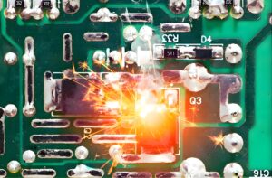
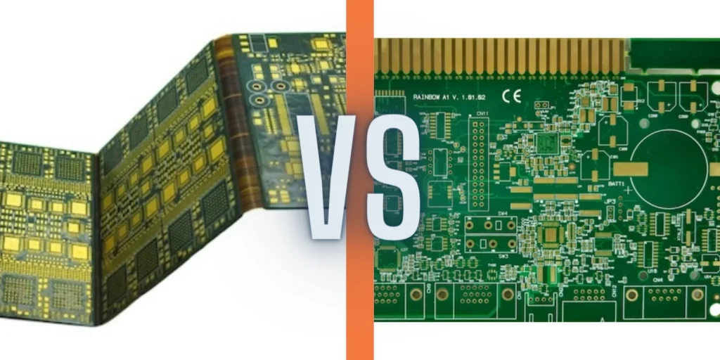
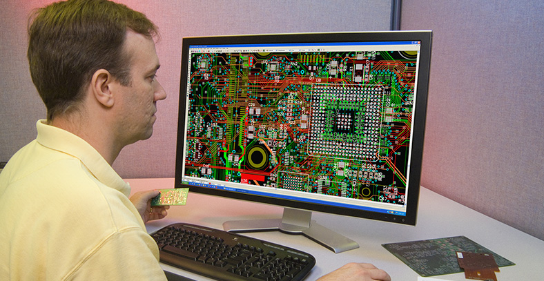
PCB short circuit is a common adverse phenomenon in electronic manufacturing, which refers to abnormal conductivity between conductive lines that should be insulated.Its causes are complex and usually involve multiple factors such as design, materials, processes, and environment.The following is a classification analysis of common reasons:
1、 Design factors
Insufficient line spacing: When high-density wiring is used, the line width/spacing design is too small, and residual copper forms a “bridge” after etching.The high-frequency signal line has not been impedance matched, resulting in potential short circuit risks caused by electromagnetic interference.
Design defects of solder pads and hole positions: The solder pad spacing is too small (such as QFN, BGA packaging), and the solder paste is prone to bridging during reflow soldering.The through-hole did not avoid the inner layer circuit, and the drilling offset caused the copper on the hole wall to come into contact with the inner layer circuit.
Gerber file error: Alignment Mark deviation between layers, resulting in misalignment and short circuit of the inner layer circuit.
Not setting sufficient electrical safety spacing (such as overlapping solder mask windows and circuits).
2、 Material issues
Substrate defect: There are conductive impurities inside the board, causing interlayer short circuits.The insulation performance of the board decreases after absorbing moisture, and ion migration occurs at high temperatures.
Abnormal quality of copper foil: Copper foil burrs or poor lamination result in residual copper spikes after etching, leading to short circuits.The adhesion between copper foil and substrate is poor, and the peeling of copper layer during processing causes circuit crossing.
3、 Manufacturing process issues
Graphic transfer and etching: Incomplete exposure and development: Insufficient etching caused by dry/wet film residue, resulting in “micro short circuits”.Improper control of etching solution concentration or time can lead to excessive side etching, resulting in rough edges of the circuit.
Drilling and hole metallization: Drill bit wear or improper rotation speed, rough hole walls resulting in copper spikes, and short circuits between holes after electroplating.Copper plating or electroplating is too thick, causing copper filling to overflow and connecting adjacent holes.
Solder mask and surface treatment: The solder mask ink coating is uneven, exposing the circuit area, and solder paste bridges during soldering.Abnormal surface treatment process results in residual conductive substances between solder pads.
SMT assembly process: The steel mesh opening is too large or the printing pressure is too high, and excessive solder paste can cause welding bridging.SMT offset causes component pins to cross adjacent solder pads, resulting in a short circuit after reflow soldering.
4、 Environment and external factors
Pollution interference: Dust or metal debris in the production environment adheres to the surface of the PCB, forming conductive pathways.The residual flux was not thoroughly cleaned, and ion migration after moisture absorption caused insulation failure.
Mechanical damage: Scratching the circuit during board splitting or assembly, damaging the solder mask and exposing the copper wire.
Excessive pressure on the test probe caused a hidden short circuit by piercing through the insulation layer.
Abnormal usage environment: The high temperature and high humidity environment accelerates the aging of the board and reduces its insulation performance.Overvoltage or overcurrent causes the circuit to burn out, and after carbonization, a conductive channel is formed.


