PCB wiring, the laying out of paths for energized signals to connect individual devices, is akin to connecting various cities through traffic by building roads. In PCB design, wiring is an important step in completing the product design, but it is also the step with the most detailed and limited skills, and even some experienced engineers have quite a headache with wiring. Here are some common rules for PCB wiring that you should master whether you are a novice or an engineer already in the industry.
Common rules for PCB routing
1. Rules for controlling the direction of the alignment
The wires at the input and output should be parallel to each other as much as possible. In PCB wiring, the alignment of adjacent layers is structured orthogonally to avoid routing different signal lines in the same direction on adjacent layers to reduce unnecessary inter-layer interference. When PCB wiring is limited by the structure (such as some backplane) to avoid parallel wiring, especially in the signal rate is high, should consider the ground plane to isolate the wiring layer, the ground line to isolate the signal lines. The alignment direction of adjacent layers is shown in the following diagram.
2. Open-loop check rule for alignment
In the PCB wiring, in order to avoid the “antenna effect” generated by the wiring, reduce unnecessary interference radiation and reception, generally do not allow one end of the floating form of wiring, otherwise it may bring unpredictable results.
3. Alignment length control rules
That is, the rule of short lines, in the design should try to make the wiring length as short as possible to reduce the interference problems caused by too long lines, especially some important signal lines, such as the clock line, be sure to place its oscillator very close to the device. For cases where multiple devices are driven, the network topology should be decided on a case-by-case basis.
4. Impedance matching check rule
The wiring width of the same network should be consistent. Variations in line width can cause uneven line characteristic impedance, and reflections can occur when the speed of transmission is high, and this should be avoided as much as possible in the design. Under certain conditions, such as connector leadouts, it may not be possible to avoid variations in line width when the BGA package leadouts are similarly constructed, and the effective length of the middle inconsistent portion should be minimized.
5. Chamfering rules
In the PCB wiring, the alignment corner is inevitable, when the alignment has a right angle corner, in the corner will generate additional parasitic capacitance and parasitic inductance. alignment corner corner should be designed to avoid sharp and right angle form, so as not to generate unnecessary radiation, while sharp and right angle form of process performance is not good. requirements of all the line and line angle should be greater than or equal to 135 °. in the alignment does require
The right angle is the best way to avoid unnecessary radiation.
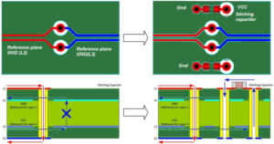
6. Device decoupling rules
A. Add the necessary decoupling capacitors to the printed circuit board to filter out interference signals from the power supply and make the power signal stable. In multilayer boards, the location of the decoupling capacitors is generally less demanding, but for dual-layer boards, the layout of the decoupling capacitors and the way the power supply is wired will directly affect the stability of the entire system, and sometimes even the success or failure of the design.
B. In a dual-layer board design, the current should generally be made to filter through the filter capacitor before it is made available to the device. c. In high-speed circuit design, the correct use of decoupling capacitors is related to the stability of the entire board.
7. 3W rule
To reduce crosstalk between lines, you should ensure that the line spacing is large enough, when the line center spacing is not less than 3 times the line width, then you can maintain 70% of the electric field does not interfere with each other, known as the 3W rule. To achieve 98% of the electric field not interfering with each other, a spacing of 10W can be used.
8. Ground loop rules
The minimum loop rule, that is, the signal line and its loop to form the smallest possible ring area, the smaller the ring area, the less external radiation, the less interference received from the outside world.
9. Mask protection
corresponding to the ground loop rules, in fact, to minimize the signal loop area, mostly seen in some of the more important signals, such as clock signals, synchronization signals; for some particularly important, particularly high frequency signals, should consider using copper shaft cable shielding structure design, that is, the line laid up and down the left and right ground line isolation, but also to consider how to effectively make the shield ground and the actual ground plane effectively The combination of
10. Resonance rules for alignments
Mainly for high-frequency signal design, that is, the wiring length must not be an integer multiple of its wavelength to avoid resonance phenomena.

