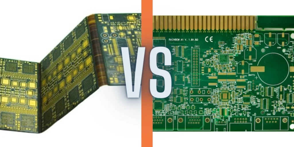
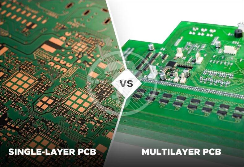
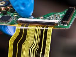
PCBs are made by handling a variety of complex process lines and different types of components. PCBs are also very complex, including single-layer, double-layer, and even multi-layer structures. Production methods will vary at different levels. To date, many types of circuit boards have been developed. Printed circuit boards can also be classified according to their rigidity. There are rigid boards (rigid boards), flexible boards (FPC) and rigid-flexible boards. The PCB rigid board is generally used more often. Usually, PCB circuit boards are divided into several layers based on the number and thickness of conductive copper foil. They can be divided into single-layer boards, double-layer boards, multilayer boards and double-sided boards. They also have different structures. Rigid PCB board suppliers will introduce their different properties.
PCB single-layer construction: This is the simplest structure for flexible boards and is usually made from raw materials purchased with substrate + clear glue + copper foil, while protective film + clear glue is a separate raw material purchased; first, the copper foil needs to be processed by etching and other processes to obtain the desired circuitry. The protective film is drilled to expose the corresponding pad. After cleaning, the two are bonded together by rolling and then gold or tin plated on the exposed pads. Protect the tin to prepare the large board, which then needs to be stamped into a small board with the appropriate shape.
PCB double layer board structure: When the circuit is too complex for single layer wiring or requires copper foil grounding, a double layer board or multi-layer board is required.
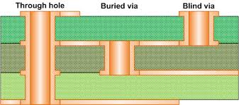
PCB multilayer structure: The most typical difference between multilayer and single-layer boards is the addition of a through-hole structure to connect the layers of copper foil. The first process of general substrate+transparent+copper foil is to create through-hole; first, holes are drilled in the substrate and copper foil, then a certain thickness of copper is plated after cleaning to complete the through-hole. The subsequent manufacturing process is almost the same as for single-layer boards.
PCB double-sided construction: Pads are provided on both sides of the double-sided board, mainly for connecting to other boards. Although the structure is similar to that of a single-layer board, the manufacturing process is quite different. Its raw materials are copper foil, protective film + transparent adhesive. First, it is necessary to drill holes in the protective film according to the requirements of the pad location, and then paste the copper foil. Then the pads and leads are etched out, and then another drilled hole is applied to the protective film.
While these flexible circuit boards have different types of structures, such as multilayer flexible PCBs, many of the manufacturing processes are similar, with just a few basic areas where different processes have been added to correspond to different areas.
These are the different structures of the PCB from the PCB manufacturer. We hope it will be helpful.
