Transistor scaling is reaching a tipping point at 3nm, where nanosheet FETs will likely replace finFETs to meet performance, power, area, and cost (PPAC) goals. A significant architectural change is similarly being evaluated for copper interconnects at 2nm, a move that would reconfigure the way power is delivered to transistors.
This approach relies on so-called buried power rails (BPRs) and backside power distribution, leaving the front-side interconnects to carry signals. Intel announced it will use its PowerVia structure at its 20Å generation (2nm equivalent), and other chip manufacturers are evaluating similar schemes.
Chipmakers also are likely to replace copper at some levels with ruthenium or molybdenum as soon as the 2nm node. Other, more modest changes will extend copper damascene interconnects using low-resistance via processes, alternative liners, and fully aligned via approaches.
Much of the optimization happens around the weak links in the chain — the contact (metal 0), metal 1, and vias, where RC delays are most likely to slow the chip down. “For via filling, conformal deposition of barrier, seed, and via metal may be supplanted by barrier-less deposition and bottom-up fill of cobalt, and perhaps even ruthenium,” said Ajit Paranjpe, CTO of Veeco.
Interconnect challenges begin at lithography, where EUV is employed at throughout 5nm process, contributing significantly to cost.
EUV and BEOL patterning
Only a handful of mask levels require EUV lithography at the 7nm node, but this changes to between 15 and 18 levels at 5nm (about 30nm metal pitch). In lithography, an increasing concern is edge-placement errors (EPEs) due to imprecisely aligned features. Robert Socha, an ASML fellow, emphasized the need to control and reduce contributors to EPEs at the 5nm node. A critical contributor is overlay errors, with overlay budget of only 2.5nm (5 silicon atoms wide) at the 5nm node.
“We have seen the overlay element of the EPE budget shrinking the fastest with higher within-field variation,” said Andrew Cross, director of process control solutions at KLA. “This leads to higher optical overlay sampling, improved overlay measurement techniques, and use of SEM-based overlay measurements after resist development and after etching, which calls for synergy between optical and e-beam based tools.”
Via optimization
A key strategy in extending copper technology involves eliminating the barrier metal, TaN, at the copper via bottom. One way this can be accomplished is by depositing a self-assembled monolayer (SAM) film selectively, depositing the TaN by atomic-layer deposition (ALD) along the sidewalls, and finally removing the SAM and filling with copper. At IITC, TEL described such a process using dual damascene integration [1], and comparing two self-assembled monolayers (A and B). Following TaN barrier ALD, the SAMs were evaporated, followed by copper electroless deposition (ELD) in the via (see figure 1). After via prefill, a ruthenium liner was deposited by CVD on the trench sidewalls, followed by copper ionized PVD fill. With SAM B, the results showed no Ta (EDX) on the via bottom. A key aspect of any SAM is that it can withstand the process temperature of ALD, which is around 350° C.
Chipmakers are increasingly looking to SAM processes, whether by CVD or spin-coat, as critical to reducing overall resistance and extending copper damascene processes to the 2nm node.
Another strategy that reduces the volume of barrier metal (TaN) at the via bottom involves a transition from PVD TaN to ALD TaN, which is more conformal and results in a thinner, more continuous film. ALD TaN is expected to be widely implemented at the 5nm node, perhaps with SAM processes.
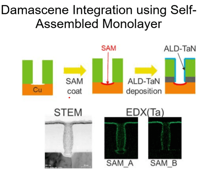
Fig. 1: In this self-assembled monolayer (SAM) process, a film masks the via bottom during ALD of the barrier and copper seed. The SAM is then removed by vaporization at 325°C, followed by copper fill. Source: TEL/IITC
Fully aligned vias, selective deposition
The idea behind fully aligned vias (FAVs) is to reduce the impact of edge placement errors between vias and lines, which lead to device failures and long-term reliability issues. Since the 32nm node, chipmakers have been employing self-aligned methods using TiN hard masks to align interconnects to the level below. In fully aligned vias, the via below and above are registered. There are two methods to achieve FAVs, by etching some copper from the lines below and then patterning and depositing the via, or by depositing a dielectric film selectively on the low-k dielectric, followed by via patterning.
Engineers from IBM and Lam Research presented a fully aligned approach uses selective dielectric deposition in a simplified overall process [2]. According to the group, FAV integration can enable 70% lower resistance and a 30% increase in via contact area while maintaining via-to-line reliability (see figure 2). Using 32nm-pitch test structures of copper and low-k dielectric (SiCOH), the team used a wet chemistry to recess the copper, liner, and barrier.
“[The recess etch], when combined with an etch-selective dielectric cap, acts as a via guiding pattern, mitigating overlay and critical dimension (CD) induced edge placement errors,” according to IBM. A selective aluminum oxide film was deposited by CVD on the low-k and acts as a partial etch stop. Key to the success of the process is high selectivity with limited lateral overgrowth of dielectric film, and no resistance decrease or variation compared to its standard FAV process. IBM stated that a further advantage is the lower aspect ratio of the metal lines (because the recess is shallow), which eases copper filling.
At this time, it is unclear how popular fully aligned via approaches will become. “The question is in what form — at what levels and at what pitch will (fully aligned vias) be required?” asks Zsolt Tokei, an Imec fellow. He noted that while both recess etch and selective deposition approaches have their pros and cons, the key issue is defectivity and driving up the yield on new processes. Even so, with the ever-smaller EPE tolerance at the 3nm and 2nm nodes, approaches like FAV likely will become more compelling.
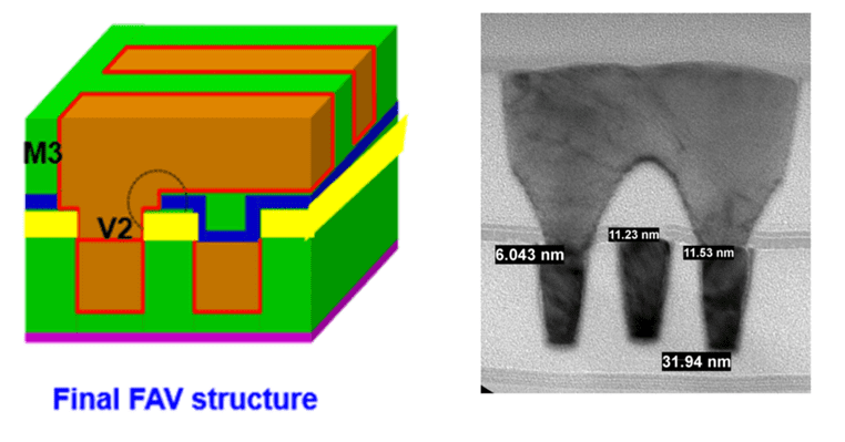
Fig. 2: A selective deposition process was used to fabricate a two-level fully aligned via for a 5nm node. Source: IBM/IITC
Selective deposition, also known as area-selective deposition (ASD), has been around for decades, but it’s only in recent years that it has made the step from lab to fab. For ASD, the “killer app” proved to be deposition of cobalt caps on copper lines, which enables superior control of electromigration over traditional silicon nitride caps. That technique was adopted by some companies at the 10nm node. Together with a cobalt liner underneath the copper (liners are also called nucleation layers or glue layers because they enable metal adhesion), cobalt encases the copper in this scheme.
Selective ALD processes perform best when the goal is to deposit metal on metal, or dielectric on dielectric. Depending on the equipment vendor, different chemical mechanisms may be used to keep the deposition selective and prevent deposition where it is not wanted. For contact metallization, selective tungsten deposition potentially reduces resistivity dramatically through improved filling and potentially eliminating the TiN barrier altogether (see figure 3). By eliminating sidewall barriers and liners, selective tungsten also allows a clean metal-to-metal interface for lower overall resistance. According to Applied Materials, a 40% reduction in resistance is possible.
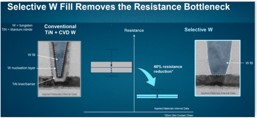
Fig. 3: Selective tungsten bottom-up fill provides a pathway to eliminate barrier and liner layers, improving contact and resistance. Source: Applied Materials
Cobalt and tungsten
Up until the 14nm or 10nm technology node, tungsten has remained the mainstay for making electrical contact to the metal/polysilicon gate and the source and drain silicide regions on transistors. In recent years, cobalt contacts were adopted with a thin TiN barrier. Likewise in lines or vias, the thinner barrier, along with the shorter mean free path of cobalt (10nm vs. 39nm for copper), results in lower resistivity in small wires (with longer electron path, scattering increases net resistance).
Intel was the first company to use cobalt in production at the contact level, and indeed the integration issues with cobalt may have been a partial cause of problems with Intel’s 10nm delays. Nonetheless, several chipmakers made the transition to using cobalt in production processes for contacts, but also as a liner and capping material in copper interconnects.
The liner metal critically affects the fill quality of the copper in scaled interconnect lines. In an invited presentation at IITC, IBM demonstrated improved electromigration performance using a new liner, cobalt-doped ruthenium by CVD [3], relative to CVD cobalt and CVD ruthenium liners in 36nm metal structures. IBM determined that the new liner gives better EM resistance because the cobalt in the ruthenium liner suppresses diffusion along grain boundaries caused by the cobalt cap on copper. PVD copper with reflow at low temperatures (250°C) is becoming mainstream for dense interconnects, while electroless copper or ECD are used at global levels.
The next metal: Ru or Mo?
It appears that at the 1nm node (20nm metal pitch), a change from copper to an alternative metal — ruthenium or molybdenum — will become necessary, at least for some levels. Interestingly, both molybdenum and ruthenium are being explored as word line replacements for tungsten in 3D NAND flash transistors.
For the industry’s choice to replace copper, resistance at scaled features is the paramount metric. Also critical is EM resistance, which is tied to long-term reliability. Much of the advantage of ruthenium, molybdenum, and cobalt, is the potential to eliminate liners, affording more trench or via volume to be occupied by the main metal. Reflow or laser annealing may be used to maximize grain size.
“For metal lines, ruthenium is a likely replacement. While the bulk resistivity of ruthenium is 7 µohm-cm, the effective resistivity of a 20nm ruthenium film deposited with traditional sputtering is >11 µohm-cm,” said Veeco’s Paranjpe. “Thus, alternative methods such as ion beam deposition, which offers greater control over the crystalline texture and grain size, are being explored.”
Ruthenium is attractive as a next-generation interconnect because of its low resistivity, high melting point, resistance to attack from acids, and extremely low potential for corrosion.
Molybdenum precursors, in contrast, are an order of magnitude less expensive than ruthenium. Neither likely will be needed before the 2nm node.
“Molybdenum is definitely cheaper, so if you’re a fab manager you will be happier,” said Imec’s Tokei. “But if you’re an engineer, you need to have all the data available to make a decision between materials, and we do not have a full data set yet.”
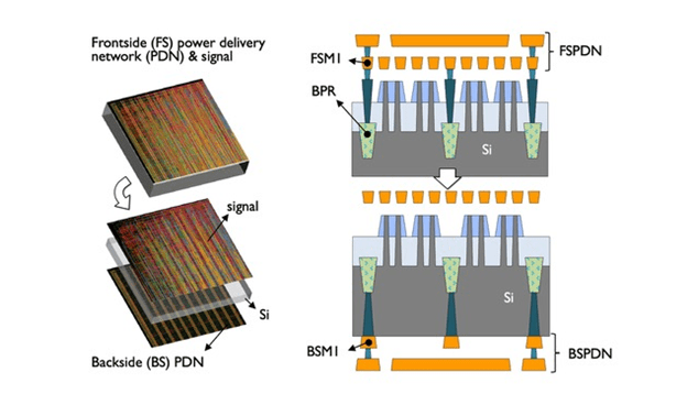
Fig. 4: By building a rail from the transistor’s isolation region through the silicon wafer, transistor power delivery (backside) is separated from signal delivery (frontside). Source: Imec
Buried power rails
The combination of BPR and backside power distribution (BPD) essentially takes power and ground wires, which previously were routed through the entire multi-level metal interconnect, and gives these a dedicated network on the wafer backside (see figure 4). This reduces voltage (IR) drop.
“In conventional interconnect, you have to optimize on metal 0 and metal 1 for both power and signals, so the power drives a tall interconnect and the signal drives a skinny interconnect. You end up with a tradeoff, which is not optimal for either,” explained Tokei. “By routing the power to the backside, there will be tall, relatively wide interconnects there, and you’re left with signal and clock on the front with relatively skinny, resistive lines, and you significantly gain route-ability.” He noted that thermal management is being evaluated carefully for these new structures.
Many challenges exist regarding BPRs and BPDs, including how to build the buried power rail, how to connect the power distribution network to the power rail, and how to transfer power from the power rail to the transistor. These decisions will determine the integration schemes and the ultimate power and scaling gains.
Mehul Naik, managing director of advanced product technology development at Applied Materials, said fabrication challenges will vary, depending on the scheme, and can include high-aspect-ratio metal fills, metal and dielectric choices, and wafer thinning through backside grinding and CMP, among others.
Intel announced it will use its PowerVia at its 20Å generation (2nm), which it aims to have in high-volume production in 2024. Semiconductor Engineering discussed PowerVia with Intel’s Ann Kelleher, senior vice president and general manager of technology development, and asked how it differed from other approaches under development. “Buried power rail, at the highest level, is the same general theme,” Kelleher said. “However, it differs in how it’s achieved. We’re delivering the power from the back of the wafer to the transistor. Buried Power Rail is basically getting it from the front side, so you have a different architecture in achieving that. It is the key difference.”
Notably, Intel’s PowerVia appears to connect at the contacts, whereas Imec’s power rail is embedded in the STI (shallow trench isolation).
David Fried, vice president of computational products at Lam Research, likens the buried power rail approach to a basement in a house. “If you use a basement analogy, there will need to be a stairwell on each side,” he said. “You now have the ability to access the items on the ground floor from both sides instead of just one. This can open a whole new design dimension when you can access the transistors from underneath or from above. It’s a huge change.”
While this shift to building access to transistors on the wafer front and back will require many process and design innovations, the fact that backside power would still have planar level-by-level construction builds on existing industry know-how.
“This is one of the technologies I’m fairly optimistic about,” said Fried. “It’s the innovations that are difficult and multifaceted, but at their core they’re proven. So a buried power rail is just another two-dimensional level on a three-dimensional flow. It’s still planar processing, so it bears similarity to everything we already do. Putting it together and making it work is really, really difficult, but at its core it’s not as revolutionary as some other options.”
Process innovations in metallization, dielectrics, and CMP will be required. “When you take the power rail and connect it to the device, how do you make sure the interfaces are clean enough and how do you reduce power losses in that transfer? Pre-clean and integration with void-free low-resistivity metals will be very important,” Applied Materials’ Naik said. “High quality, lower thermal budget dielectrics (≤400°C) will be required, as these processes occur after the front-side device, including metallization, has been fabricated.”
Founded in 2015, The company takes PCB sample manufacturing as the entrance, and has the ability of fast delivery of high-end samples and small and medium-sized batches. Through the whole value chain services such as PCB manufacturing, BOM purchasing and PCB assembly, we provide customers with vertically integrated one-stop solutions for their products. We continue to contribute to the continuous innovation and development of China’s electronic technology, in order to build a first-class electronic product design and manufacturing outsourcing service provider. Pursue the material and spiritual happiness of all staff and make contributions to the progress and development of mankind and society.
We offer professional design solutions covering all aspects of PCB and PCBA layout, including the following board technologies.
Include:
1.PCB design: free laminated design and impedance calculation.
2.PCB manufacturing :PCB board making capacity of 1-48 layers, blind hole, copper thickness up to 12 ounces
3. Component purchase :BOM purchase within 3 days
4.PCB assembly: urgent sample and batch assembly processing, only 1-3 days
5. Functional testing
6. Electronic assembly global logistics
7. Single, double-sided, multi-layer board
8. Rigid circuits, flexible circuits and rigid-flexible circuits.
Please email us to get a quote right away: sales@fastturnpcbs.com
Telephone number: 15018735409
