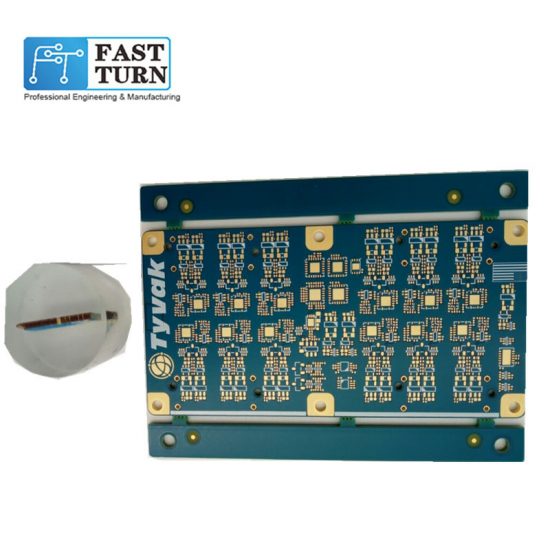
In general there are two main rules to follow for stacked design:
1. Each alignment layer must have an adjacent reference layer (power or ground);
2. The adjacent main power and ground layers are to be kept at a minimum distance to provide a large coupling capacitance.
Here is an example of a stack from two to eight layers:
I. Stacking of single-sided PCBs and double-sided PCBs
For two-layer boards, stacking is no longer an issue due to the low number of board layers. Controlling EMI radiation is mainly considered in terms of wiring and layout;
The EMC problem is becoming more and more prominent for single-layer and double-layer boards. The main reason for this phenomenon is due to the large signal loop area, which not only generates strong electromagnetic radiation, but also makes the circuit sensitive to external interference. The easiest way to improve the electromagnetic compatibility of your circuit is to reduce the area of critical signal loops.
Critical signals: From an electromagnetic compatibility perspective, critical signals are primarily those that generate strong radiation and those that are sensitive to the outside world. Signals that generate stronger radiation are typically periodic signals, such as the low bits of a clock or address. Signals that are sensitive to interference are those analog signals with low levels.
Single and double boards are typically used in low frequency analog designs below 10KHz:
1) Radial alignment of the power supply on the same layer and minimizing the sum of the line lengths;
2) Walk the power and ground lines close to each other; lay a ground line by the critical signal line, and this ground line should be as close to the signal line as possible. This creates a smaller loop area and reduces the sensitivity of differential mode radiation to external interference. When a ground is added next to the signal line, a loop with the smallest area is formed, and the signal current will definitely take this loop instead of other ground paths.
3) In case of a double layer circuit board, you can lay a ground line along the signal line on the other side of the board, immediately below the signal line, one line as wide as possible. This creates a loop area equal to the thickness of the board multiplied by the length of the signal line.
Two, four-layer stacking of panels
1. SIG-GND (PWR)-PWR (GND)-SIG;
2. GND-SIG(PWR)-SIG(PWR)-GND;
For both of the above stack designs, the potential problem is for the traditional 1.6mm (62mil) board thickness. The layer spacing will become large, which is not only detrimental to impedance control, inter-layer coupling and shielding; in particular, the large spacing between power ground layers reduces board capacitance and is detrimental to noise filtering.
For the first option, it is usually applied when there are more chips on the board. This solution gives better SI performance, not so good for EMI performance, which is mainly controlled by the alignment and other details. The main attention: the ground layer is placed in the most dense signal layer of the connected layer, which is conducive to the absorption and suppression of radiation; increase the board area, reflecting the 20H rule.
For the second option, it is usually used when the chip density on the board is low enough and there is enough area around the chip (to place the required power supply copper cladding). The outer layers of the PCB are all ground layers, and the middle two layers are both signal/power layers. Signal layer of the power supply with a wide line alignment, which can make the path of the power supply current impedance is low, and the signal microstrip path impedance is also low, but also through the outer layer of ground shielding the inner layer of signal radiation. From an EMI control perspective, this is the best 4-layer PCB structure available.
Main notes: the two middle signal and power mixed layers should be spaced apart, and the alignment direction should be vertical to avoid crosstalk; the board area should be properly controlled to reflect the 20H rule; if the alignment impedance is to be controlled, the above scheme should be very carefully arranged with the alignment underneath the power and grounded copper laying islands. In addition, the copper layouts on the power or ground layers should be interconnected together as much as possible to ensure DC and low frequency connectivity.
Three, six-panel stacking
For designs with higher chip densities and higher clock frequencies a six-layer board design should be considered with the recommended stacking method:
1. SIG-GND-SIG-PWR-GND-SIG;
For this scheme, this stacked layer scheme gives better signal integrity, the signal layer is adjacent to the ground layer, the power layer and ground layer are paired, the impedance of each alignment layer can be better controlled, and both ground layers are good at absorbing magnetic lines. The power and ground layers are intact and can provide a good return path for each signal layer.
2. GND-SIG-GND-PWR-SIG -GND;
For this scenario, which is only suitable if the device density is not very high, this stack has all the advantages of the above stack, and the top and bottom ground planes are more complete so it can be used as a better shield. It should be noted that the power supply layer to be close to the non-main component side of the layer, because the bottom layer of the plane will be more complete. Therefore, the EMI performance is better than the first option.
Summary: For a six-layer board solution, the spacing between the power and ground layers should be minimized to obtain good power-to-ground coupling. However, with a 62 mil board thickness, the layer spacing is reduced, but it is not easy to control the spacing between the main power and ground layers to be small. Comparing the first option with the second, the cost of the second option is much higher. Therefore, we usually choose the first option when stacking layers. The design follows the 20H rule and the mirror layer rule.
