When designing a printed circuit board, you need to understand a few key stages on how to best design the PCB for a given application.
Knowing how to design a PCB board is a key element of any electronic circuit design process.
PCB layout and design has a significant impact on how a circuit works, so if the PCB is designed in an efficient manner, the circuit will work more reliably within its specifications.
PCB design equipment
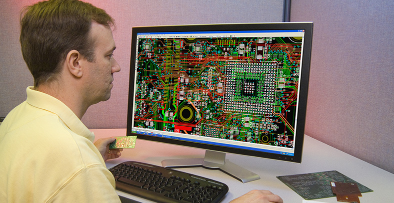
For commercial development programs, CAD, Computer Aided Design packages may be required due to complexity.
Even for students and amateurs, there are a number of very good packages that can be obtained for free at a low cost.
The old-fashioned PCB design process of using tape placed on the master drawing is a thing of the past, although it is possible that this can still be done in many very limited cases.
The functionality of PCB software varies widely. Budget or even free software provides basic functionality, while high-end packages allow for more features to be included in the design. Simulation, complex routing and more features are available.
As digital board speeds increase and RF designs reach ever higher frequencies, the ability to perform simulations is becoming increasingly important.
Circuit Schematic Capture
The first step in PCB design development is to capture the circuit schematic. This can be done in a number of ways. The circuit can be entered into a schematic capture tool. This may form part of a PCB design kit or it may be an external package whose output can be exported in an appropriate format.
In addition to performing schematic capture only, circuit simulation can also be performed at this stage. Some packages may be able to interface with simulation packages. For applications such as RF circuit design, circuit simulation allows for more optimization of the final circuit without the need to build a prototype.
When the schematic capture is complete, the electronic design of the circuit is included in the file and can be converted into what is called a “netlist”. A netlist is interconnectivity information, which is essentially the component pins and the circuit nodes or networks to which each pin is connected.

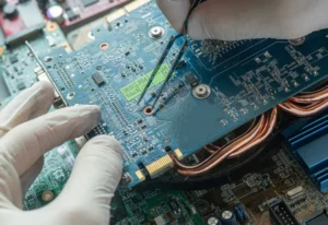
Initial PCB component placement
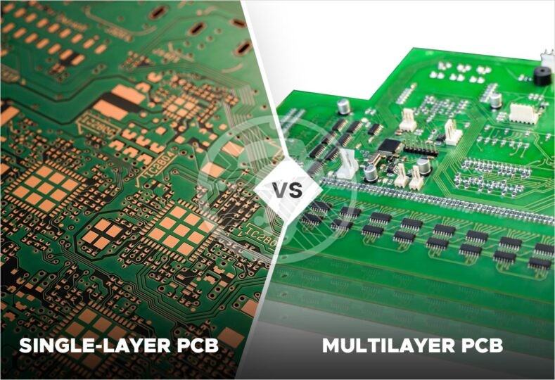
Before proceeding with detailed PCB design and layout, it is necessary to have a general idea of where the components will be located and whether there is enough space on the board to accommodate all the necessary circuitry. This will determine the number of layers required on the board and whether enough space is needed to accommodate all the circuitry.
Once a rough estimate of the space and approximate location of components has been made, a more detailed component layout can be made for the PCB design. This can take into account aspects such as the proximity of devices that may need to communicate with each other and other information related to, for example, any RF considerations.
In order for components to be incorporated into a PCB design, they must have all the relevant information associated with them. This would include the footprint of the PCB pads, all drilling information, isolation areas, etc. Often, multiple devices may share the same footprint, so it is not necessary to enter this information for each component part number. However, a library will be created in the PCB layout design system for all devices used. This allows for easy recall of previously used components.
Process Route
After completing the basic layout, the next stage of the PCB design is to wire all the connections between the components. The PCB software then routes the physical connections on the board according to the netlist on the schematic. To do this, it uses the number of layers available for connections and creates vias as needed. Usually one layer is assigned for the ground layer and another for the power layer. This not only reduces the noise level, but also makes low-source resistance connections to the power supply possible.
The process route can use a lot of computing power. This is especially true for larger designs, which may have more than three thousand or four thousand components. In cases where routing is difficult due to high component density, this can lead to significant time spent on routing.

PCB files: Gerber files and more
The information in the PCB layout photo diagram is output as a Gerber file. This format is the standard format for PCB files and is the form of CNC files used by photo plotters. In addition to the Gerber file, drill-down information is generated as well as screen print and photoresist information.
A major factor in the cost of a PCB is the drilling of holes. In any design, there are a number of holes that need to be fixed as well as any conversions
