Gold plated PCBs are widely used due to their excellent conductivity and corrosion resistance. However, the surface of the gold deposit is prone to oxidation problems when exposed for a long time or stored improperly, which not only affects its appearance but may also cause damage to its electrical performance.
1、 Oxidation mechanism of gold-plated PCB
The oxidation of gold-plated PCBs is mainly caused by chemical reactions between the metal surface and oxygen, humidity, and other pollutants in the air, resulting in the formation of oxides. These oxides usually appear in the form of dark yellow, dark gray, or gray brown spots on the surface of deposited gold, which not only affects aesthetics, but also reduces weldability and solderability, and has adverse effects on subsequent welding and electrical performance.
2、 Oxidation rate of gold-plated PCB
The oxidation rate of gold-plated PCBs is influenced by various factors, including temperature, humidity, air quality, and the length of exposure time. In general, exposed gold-plated PCBs may begin to show signs of oxidation within weeks to months. However, in environments with high temperature, high humidity, or severe pollution, the oxidation rate will significantly accelerate. Therefore, controlling the production environment and storage conditions is the key to delaying oxidation.
3、 How to prevent oxidation of gold-plated PCB
Control the production environment: Ensure that the temperature and humidity in the production workshop are within a reasonable range, and avoid accelerated oxidation in high temperature and high humidity environments. Regularly clean production equipment and workshops to reduce dust and pollutants in the air. Strictly control all aspects of the production process, such as etching, drilling, gold plating, etc., to ensure product quality.
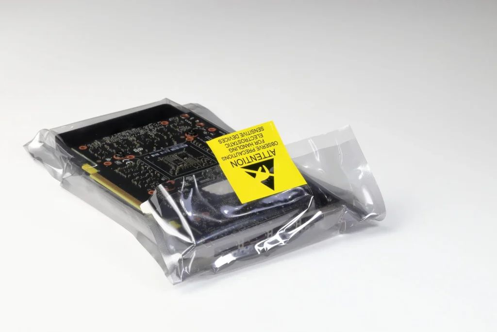
Optimize storage conditions: For gold-plated PCBs that require long-term storage, sealing measures such as sealed bags and vacuum packaging should be used to reduce contact with air and moisture. Avoid exposing the PCB to harmful chemicals such as acidic and alkaline solutions, corrosive gases, etc. The storage environment should be kept dry, ventilated, and regularly checked for storage conditions.
Reasonable PCB design: During the design phase, select appropriate boards and thicknesses, optimize circuit layout and component layout to reduce signal interference and improve circuit performance. Select the appropriate immersion thickness according to product requirements to ensure good conductivity and corrosion resistance.
Strengthen quality inspection: Real time monitoring of the production process, timely detection and resolution of problems. Conduct strict quality inspections on PCBs, including visual inspection, electrical performance testing, etc., to ensure that the products meet the requirements.
Pay attention to usage details: During use, avoid unnecessary prolonged exposure and complete welding and assembly as soon as possible. Follow the correct operating procedures to avoid physical damage or chemical contamination to the PCB.


