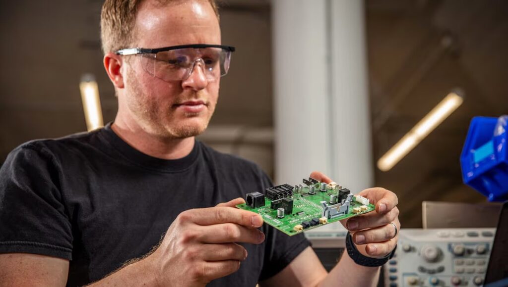
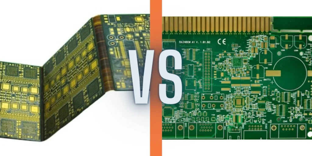
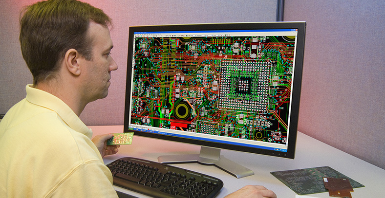
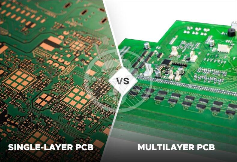
SMT (Surface Mount Technology), also known as Surface Mount Technology, is one of the key technologies in modern electronic device manufacturing. It directly attaches electronic components onto the surface of PCBs (printed circuit boards) through automated equipment, achieving efficient and high-precision assembly of electronic components. The perfection and refinement of SMT process flow are directly related to the quality and production efficiency of electronic products.
1. Solder paste printing
Solder paste printing is the first step in the SMT process, which uses steel mesh to print solder paste onto the solder pads of the PCB. The key to this step is to precisely control the amount and uniformity of solder paste to ensure that subsequent SMT components can be firmly soldered onto the PCB.
2. Component mounting
Next is the component placement process, where automated equipment will accurately place electronic components on the PCB according to the preset program. This step requires extremely high precision and speed to ensure that each component can be accurately placed in the predetermined position.
3. Reflow soldering
After completing component placement, the PCB will enter the reflow soldering process. In this process, the PCB is reflow welded and the solder paste is melted at high temperatures, firmly bonding electronic components with the PCB. The temperature curve and time control of reflow soldering are key to ensuring welding quality.
4. Quality inspection
After welding is completed, quality inspection of the PCB is required. This includes using AOI (Automatic Optical Inspection) equipment for visual inspection, as well as inspecting the internal structure of welded joints through X-ray equipment. These detection methods can timely detect and handle potential problems during the welding process, such as virtual soldering, short circuits, etc.
5. Functional testing
After passing the quality inspection, the PCB will undergo functional testing. This step aims to verify whether all components on the PCB are working properly according to the design requirements. Functional testing usually includes multiple stages such as power on testing and signal integrity testing.


