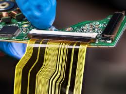
PCB wiring inspection is an important step in ensuring the performance and manufacturing feasibility of circuit boards. It is a complex and meticulous process that requires the comprehensive use of multiple inspection methods and tools to ensure the correctness and reliability of wiring.Through a strict inspection process, problems can be identified and resolved in a timely manner, improving the performance and stability of the circuit board.
Here are some commonly used PCB wiring inspection methods:
1、 Design rule check
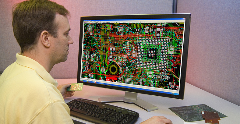
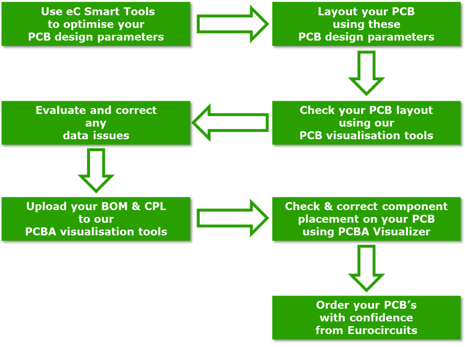
After completing the PCB wiring, the design rule checking tool should be used first to verify whether the wiring complies with the preset design rules, such as line width, line spacing, through-hole size, etc.
2、 3D simulation inspection
By utilizing the 3D simulation function of PCB design software, it is possible to perform 3D simulation inspection on wiring.
This method can visually display the layout of wiring in three-dimensional space, identify wiring conflicts, interference, and insufficient space issues, adjust and optimize wiring in a timely manner, and ensure the correctness and reliability of wiring.
3、 Signal integrity analysis
Signal integrity analysis tools can perform signal transmission simulation analysis on wiring, checking for issues such as signal delay and waveform distortion.
4、 Other inspection items
In addition to the above inspection methods, a series of specific inspections of PCB wiring are also required, including but not limited to:
Distance inspection of through holes: Ensure that the distance between through holes is reasonable and avoid mutual interference.
Width inspection of power and ground wires: Check if the width of the power and ground wires is sufficient to meet the current transmission requirements.
Key signal line inspection: Take the best measures for key signal lines, such as thickening line width, increasing protection, etc., to ensure the stability of signal transmission.
Grounding inspection for analog and digital circuits: Ensure that analog and digital circuits have independent grounding wires to avoid mutual interference.
Graphic inspection: Check whether the added graphics in the PCB will cause signal short circuits or interference.
Process line inspection: Check whether there are process lines added to the PCB board, and if necessary, carry out corresponding processing.
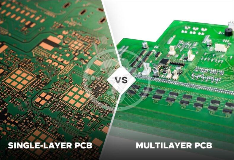
Multi layer PCB power layer outer frame edge inspection: Ensure that the outer frame edge of the power layer in the multi-layer PCB board is not reduced to avoid affecting power transmission.
