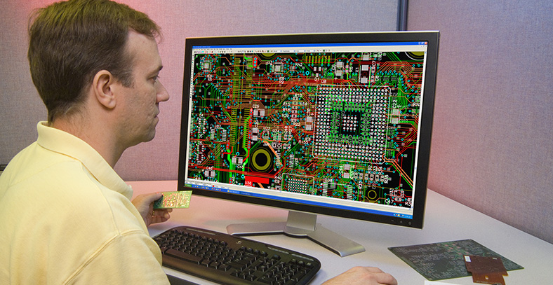
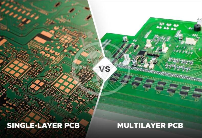
The most basic process of designing a circuit board can be divided into three major steps: the design of the circuit schematic, the generation of the network table, and the design of the printed circuit board. Whether it is the layout of the devices on the board or the alignment, etc. there are specific requirements.
For example, parallel input and output routing should be avoided as much as possible to avoid interference. Two signal lines in parallel should be isolated by adding ground if necessary, and two adjacent layers should be wired as perpendicular to each other as possible, parallel to easily generate parasitic coupling. Power and ground should be divided as far as possible in two layers perpendicular to each other. Line width, the digital circuit PCB available wide ground line to do a circuit, that is, to form a ground network (analog circuits can not be used in this way), with a large area of copper laying.

The following article explains the principles and some details of the PCB design for microcontroller control boards that need to be taken into account.
1. Component layout
In terms of component layout, components that are related to each other should be placed as close together as possible. For example, clock generators, crystal oscillators, and CPU clock inputs are prone to noise generation and should be placed closer together. For those devices that are prone to noise, small current circuits, high current circuits switching circuits, etc., should be kept as far away as possible from the logic control circuits and storage circuits of the microcontroller (ROM, RAM), if possible, these circuits can be additionally made into circuit boards, which are conducive to anti-interference and improve the reliability of the circuit work.
2. Decoupling capacitors
Try to install decoupling capacitors next to critical components such as ROM, RAM, and other chips. In fact, printed circuit board alignments, pin connections, and wiring may contain large inductive effects. Large inductors can cause severe switching noise spikes in the Vcc path. The only way to prevent switching noise spikes on the Vcc alignment is to place a 0.1uF electronic decoupling capacitor between VCC and power ground. If a surface mount component is used on the board, a chip capacitor can be used directly adjacent to the component and secured on the Vcc pin. It is best to use porcelain chip capacitors, this is because this capacitor has a low electrostatic loss (ESL) and high frequency impedance, in addition to the temperature and time of this capacitor dielectric stability is also very good. Try not to use tantalum capacitors because of its high impedance at high frequencies.
The following points need to be noted when placing the decoupling capacitors:
Connect an electrolytic capacitor of about 100uF across the power input of the printed circuit board, or better yet, a larger capacity if the size allows.
In principle, each IC chip needs to have a 0.01uF ceramic chip capacitor placed next to it. If the gap in the board is too small to fit, a 1-10 tantalum capacitor can be placed every 10 chips or so.
For components with weak immunity to interference, large current changes during shutdown, and memory components such as RAM and ROM, a decoupling capacitor should be connected between the power line (Vcc) and ground.
The leads of the capacitors should not be too long, especially the high frequency bypass capacitors should not have leads.
3. Ground design
There are many types of grounds in a microcontroller control system, including system ground, shielded ground, logic ground, analog ground, etc. Whether the ground is laid out properly will determine the board’s immunity to interference. When designing grounds and grounding points, the following issues should be considered:
Logical and analog grounds should be wired separately and not combined, connecting their respective grounds to the corresponding power ground. When designing, analog grounds should be as thick as possible, and the ground area of the lead-in should be as large as possible. In general, for the input and output analog signals, it is best to isolate them from the microcontroller circuitry via optocouplers.
When designing the printed circuit version of a logic circuit, its ground should form a closed-loop form to improve the circuit’s immunity to interference.
The ground wire should be as thick as possible. If the ground wire is very thin, the ground resistance will be higher, causing the ground potential to vary with the current, resulting in unstable signal levels and leading to a reduction in the circuit’s immunity to interference. When wiring space allows, make sure the width of the main ground wire is at least 2-3mm, and the ground wire on the component pins should be around 1.5mm.
Be careful with the choice of grounding points. When the signal frequency on the board is lower than 1MHz, the influence of electromagnetic induction between the wiring and components is minimal, while the grounding circuit forms a loop for interference, so a point of grounding should be used so that no loop is formed. When the signal frequency on the board is higher than 10MHz, the ground impedance becomes large due to the obvious inductive effect of the PCB wiring design, when the loop current formed by the grounding circuit is no longer a major problem. Therefore, multiple points of grounding should be used to minimize ground impedance.
4. Other
The layout of the power lines in addition to the size of the current to try to thicken the width of the alignment, in the PCB wiring design should also make the power lines, ground line alignment direction and data line alignment body in line with the PCB wiring design work at the end of the ground line will be the bottom of the board without the alignment of the pavement, these methods will help to enhance the circuit’s immunity to interference.
The width of the data line should be as wide as possible to minimize impedance. The width of the data line should be at least 0.3mm (12mil), and it would be better if 0.46~0.5mm (18mil~20mil) is used.
Because a single vias on a circuit board can introduce a capacitive effect of approximately 10pF, which is too much interference for high frequency circuits, the number of vias should be kept to a minimum when designing a PCB layout. In addition, too many vias can cause the mechanical strength of the board to be reduced.

