1. Process classification
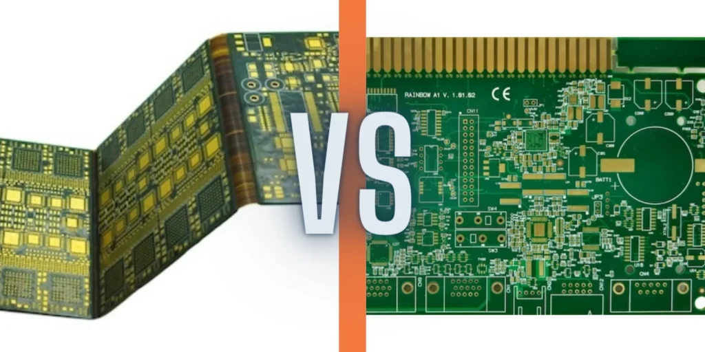
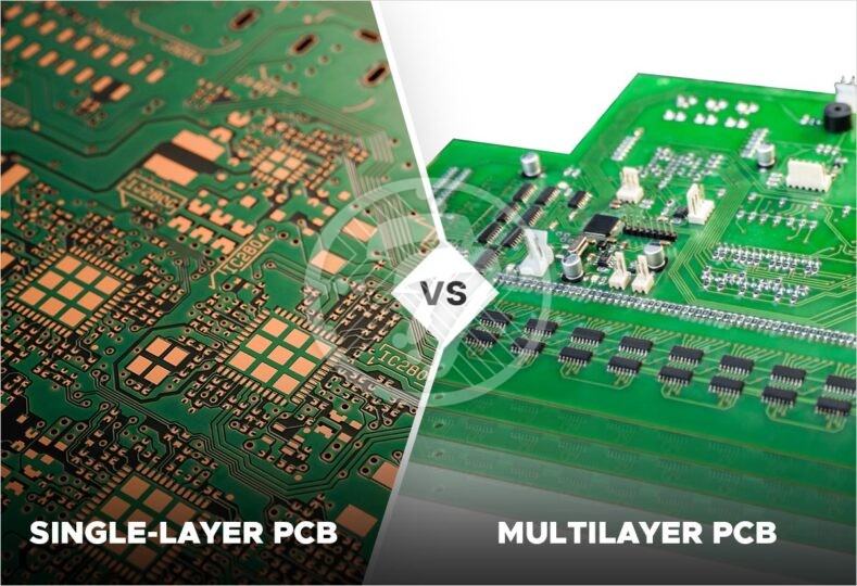
Divided into single-sided, double-sided, and multilayer boards by the number of PCB layers, these three board processes are not quite the same.
Single-sided and double-sided panels do not have an internal flow, it is basically an open-drill-follow-up process;
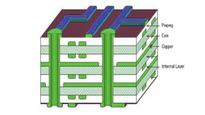
Multi-layer boards will have an inner flow
1) Single panel process flow
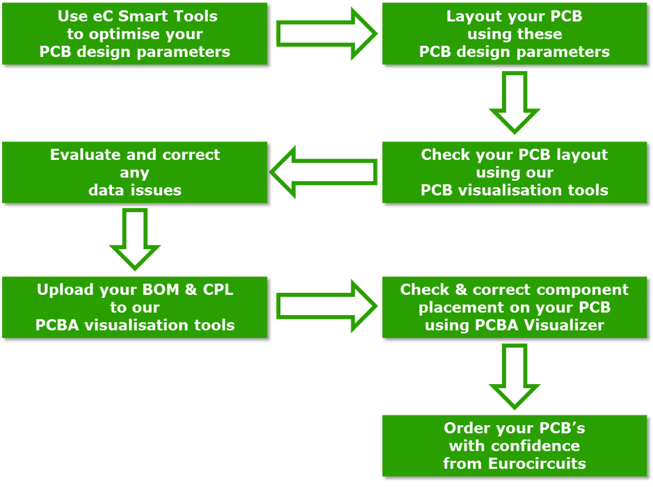
Cutting and grinding → drilling → outer layer graphics → (full board gilding) → etching → inspection → silkscreen resist → (hot air leveling) → silkscreen characters → profile processing → testing → inspection
2) Double-sided spray tin plate process
Cutting and grinding → drilling → sinking copper thickening → outer layer graphics → tinning and etching retinning → secondary drilling → inspection → silkscreen solder resist → gold-plated plug → hot air leveling → silkscreen characters → shape processing → testing → inspection
3) Double-sided nickel-gold plating process
Cutting and grinding → drilling → copper sinking and thickening → outer layer graphics → nickel and gold plating de-film etching → secondary drilling → inspection → silkscreen solder resist → silkscreen characters → shape processing → testing → inspection
4) Multilayer spray tin board process flow
Cutting and grinding → drilling positioning holes → inner layer graphics → inner layer etching → inspection → blackening → lamination → drilling → sinking copper thickening → outer layer graphics → tinning, etching de-tinning → secondary drilling → inspection → silk-screening resist → gold-plated plugs → hot air leveling → silk-screening characters → shape processing → testing → inspection
5) Nickel-gold plating process for multilayer boards
Cutting and grinding → drilling positioning holes → inner layer graphics → inner layer etching → inspection → blackening → lamination → drilling → sinking copper thickening → outer layer graphics → gold plating, de-filming etching → secondary drilling → inspection → silkscreen resist → silkscreen characters → shape processing → testing → inspection
6) Multilayer sink nickel gold plate process
Opening and grinding → drilling positioning holes → inner layer graphics → inner layer etching → inspection → blackening → lamination → drilling → sinking copper thickening → outer layer graphics → tinning, etching retinning → secondary drilling → inspection → silkscreen resist → chemically sunk nickel gold → silkscreen characters → shape processing → testing → inspection
2. Inner layer production (graphic transfer)
Inner layer: cutting board, inner layer pre-processing, lamination, exposure, DES linkage
(1) Opening and cutting the board
Cutting (cutting board – Board Cut)
Purpose: To cut large material into MI s specified size according to order requirements (according to the requirements planned by the pre-production design, the substrate material is cut into the size required for the job)
Main raw materials: substrate, saw blade
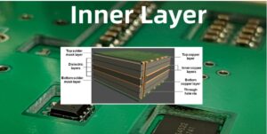
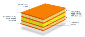
The substrate is made of copper and insulation laminate, which is available in different thicknesses according to the requirements, and can be divided into H/H, 1OZ/1OZ, 2OZ/2OZ and other types according to the copper thickness
Caution:
a. Avoid the quality of the board edge bari, cut and round the edges
b. Bake the cut board before sending it down the process, taking into account the effect of shrinkage
c. Cutting must be consistent with mechanical orientation
*Grinding/Rounding: Remove the glass fibers left by the right angles of the four sides of the board during the opening by mechanical grinding to reduce the scuffing/scratching of the board surface during the post-production process, which causes hidden quality problems
*Baking: Baking removes water vapor and organic volatiles, releases internal stress, promotes cross-linking reactions, and increases the dimensional stability, chemical stability, and mechanical strength of the board
* Control points:
a Board: spar size, board thickness, board type, copper thickness
b. Operation: baking time /temperature, stack height
(2) Inner layer production after board cutting
Role and principle
After grinding plate roughening of the inner copper plate, dried by grinding plate, paste the dry film IW, using UV light (ultraviolet) irradiation, the exposed dry film hardened, can not be dissolved in the presence of weak alkali, can be dissolved in the presence of strong alkali, while the unexposed part can be dissolved off in the presence of weak alkali, the inner line is the use of the characteristics of the material to transfer the graphics to the copper surface, that is, image transfer
Detail :(The photoreceptor initiator in the exposed area of the resist absorbs photons and breaks down into free groups, which trigger cross-linking of the monomers to form a spatially reticulated macromolecular structure insoluble in dilute alkali, while the unexposed portion is soluble in dilute alkali because no reaction occurs. The image is transferred from the negative to the substrate by using the different solubility properties of the two in the same solution).
Line graphics require high temperature and humidity conditions, typically requiring a temperature of 22+/-3°C and a humidity of 55+/-10% to prevent distortion of the film. High requirements for dustiness in the air, as the density of produced lines increases and the smaller the lines, the dust content is less than or equal to 10,000 levels or more
Material introduction
Dry film: Dry film is a water-soluble resist film with a thickness of 1.2mil, 1.5mil and 2mil etc. It is divided into three layers: polyester protective film, polyethylene septum and photographic film. The role of polyethylene diaphragm is when the rolled dry film in transport and storage time, to prevent its soft film resist and polyethylene protective film surface adhesion. The protective film prevents oxygen from penetrating into the resist layer and reacting accidentally with the free radicals therein to cause a photopolymerization reaction, while the dry film without polymerization is easily flushed out by the sodium carbonate solution
Wet film: Wet film is a one-component liquid photographic film, mainly composed of high-sensitivity resins, photographic agents, colorants, fillers and a small amount of solvents, with a production viscosity of 10-15 dpa.s. It is resistant to corrosion and plating.
Introduction to the process
Dry film imaging method with the following production process
Pre-treatment — lamination — exposure — development — etching — de-lamination
Pre-treatment (Pretreate)
Purpose: To remove contaminants such as grease oxide layer from the copper surface and increase the roughness of the copper surface for the subsequent lamination process
Main raw material: brush wheel
Pre-processing method:
(1) Sandblasting and grinding method (2) Chemical treatment method (3) Mechanical grinding method
Basic principle of the chemical treatment method: chemical substances such as SPS and other acidic substances are used to evenly bite the copper surface to remove impurities such as grease and oxides from the copper surface
Chemical cleaning: remove oil, fingerprints and other organic dirt from the copper surface with an alkaline solution, then remove the oxide layer and the protective coating on the original copper substrate that did not prevent the copper from being oxidized with an acidic solution, and finally microetch to obtain a fully roughened surface with excellent adhesion properties to the dry film.
Control points
a. Grinding plate speed (2.5-3.2mm/min)
b. Abrasion width (500# needle brush abrasion width: 8-14mm , 800# non-woven abrasion width: 8-16mm), water abrasion experiment, drying temperature (80-90°C)
l Lamination (Lamination)
Purpose: To apply a resist dry film to the copper side of a treated substrate by hot pressing
Main raw materials: Dry Film, solution visualization type, semi-aqueous solution visualization type, water-soluble dry film mainly by its composition contains organic acids, will react with strong alkali to make it organic acids, who can be dissolved off
Principle: reel dry film (lamination): first peel off the polyethylene protective film from the dry film, and then under the conditions of heating and pressure will be dry film resist pasted on the copper-clad board, the resist layer in the dry film is heated and softened, the fluidity increases, with the help of the pressure of the hot press reel and the role of the binder in the resist to complete the film.
The three elements of reel dry film: pressure, temperature, transfer rate
Control points
a. Film speed (1.5+/-0.5m/min), film pressure (5+/-1kg/cm2), film temperature (110+/-10°C), and exit temperature (40-60°C)
b. Wet film coating: ink viscosity, coating speed, coating thickness, pre-bake time/temperature (5-10 minutes for the first side, 10-20 minutes for the second side)
l Exposure (Exposure)
Purpose: To transfer the image from the original negative to the photographic plate by the action of a light source
Main raw materials: the negative used in the inner layer of the negative is negative, i.e. the white translucent part of the polymerization reaction, the black part is not translucent, no reaction occurs, the negative used in the outer layer is positive, the opposite of the negative used in the inner layer of the dry film exposure principle: in the exposure area resist in the photographic initiator absorbs photons decomposition into free radicals, free radicals trigger the cross-linking reaction of monomers to produce insoluble in dilute alkali space network macromolecular structure
Control points: alignment accuracy, exposure energy, exposure light scale (6-8 levels of cover film), dwell time
Developing
Purpose: To wash out the dry film without chemical reaction by the action of alkali
Main raw material: Na2CO3
The dry film without polymerization is washed off, while the dry film with polymerization is retained on the board as a resist layer for etching
Developing principle: The reactive groups in the unexposed portion of the photographic film react with dilute alkali solution to form soluble substances that dissolve the unexposed portion, while the exposed portion of the dry film is not dissolved
Etching
Purpose: To etch away the copper that is exposed after development using a chemical solution to form the inner line pattern
Main raw material: etchant solution (CuCl2)
Inner etching principle: the inner layer of the graphic transfer process, D/F or ink is used as a resist etching, there is anti-plating or anti-etching purposes, so most choose acid etching (dry film / wet film to cover the surface of the circuit graphics to prevent copper etching: other exposed copper on the substrate do not want to be removed by chemical reaction, so that it forms the desired line graphics, line graphics etching is completed and then retired with sodium hydroxide solution dry film / wet film)
Frequently asked questions: poor etching, over-etching, young lines, open circuits, short circuits
Control points:
a. Etching: speed, temperature (48-52°C), pressure (1.2-2.5 Kg/cm2)
b. Decontamination: 44-54°C, 8-12% NaOH solution
Strip
Purpose: Use strong alkali to strip off the resist layer protecting the copper surface, exposing the line graphics
Main ingredient: NaOH

