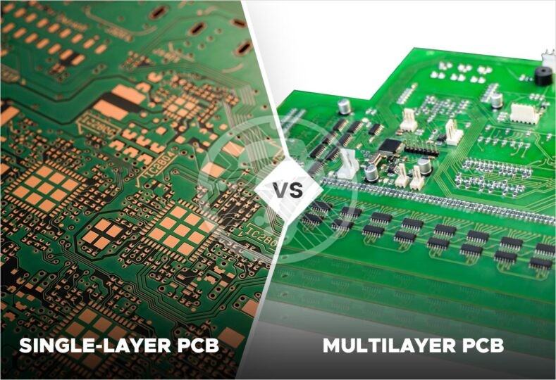
1. The reason why you should try not to split across power supplies when wiring is that when a signal crosses different power layers, it has a long return path and is susceptible to interference. Of course, it is not strictly required not to cross the power split, for the low-speed signal is possible, because the interference generated compared to the signal can not care. For high-speed signals should be carefully checked, try not to cross, you can adjust the power supply part of the alignment. (This is said for multilayer boards with multiple power supplies)
2. Some single boards have external input and output interfaces, such as serial port connectors, network RJ45 connectors, etc. If their grounding is not properly designed, it can also affect normal operation, such as network interconnections with error codes, packet loss, etc., and can be a source of external electromagnetic interference, sending noise from the board to the outside. Generally speaking will be a separate piece of independent interface ground, and the signal ground connection using a thin cable connection, you can string 0 ohms or a small resistance resistor. The thin line can be used to block the signal ground noise over the interface ground to come. Likewise, the filtering of the interface ground and interface power should be carefully considered.
3. Common grounding symbols: PE,PGND,FG-protection ground or enclosure; GND-working ground; DGND-digital ground; AGND-analog ground; LGND-lightning protection ground.
4. How to choose a PCB board. Selecting a PCB board must strike a balance between meeting design requirements and mass production availability and cost. Design requirements include both electrical and mechanical components. This material issue is usually more important when designing very high speed PCBs (frequencies greater than GHz). For example, the dielectric loss of the FR-4 material commonly used today can have a significant impact on signal attenuation at frequencies of several GHz and may not be suitable. In electrical terms, it is important to note whether the dielectric constant and dielectric loss are compatible at the frequency for which it is designed.
5. The basic idea of how to avoid high-frequency interference is to minimize the interference from the electromagnetic field of high-frequency signals, also known as Crosstalk. This can be achieved by increasing the distance between the high speed signal and the analog signal, or by adding ground guard/shunt traces next to the analog signal. Note also the noise interference from the digital ground to the analog ground.
6 Why differential pairs should be wired close together and parallel, and how differential pairs should be wired should be appropriately close together and parallel. This is because the spacing affects the value of differential impedance, which is an important parameter in the design of differential pairs. Parallelism is also required to maintain the consistency of the differential impedance. If the two lines are far apart and close together, the differential impedance will be inconsistent, which will affect signal integrity and timing delay.
7. Whether or not adding a test point will affect the quality of the high-speed signal depends on how the test point is added and how fast the signal actually is. Basically, an additional test point (not using the existing via or DIP pin as a test point) may be added to the line or a small section of wire may be pulled out from the line. The former is equivalent to adding a small capacitor to the line, while the latter is an additional branch. Both cases will have more or less impact on the high-speed signal, and the degree of impact is related to the signal frequency speed and the edge rate (edge rate). The size of the impact can be learned through simulation. In principle, the smaller the test point the better (and, of course, the requirements of the test machine) and the shorter the branch the better.

