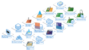
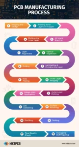
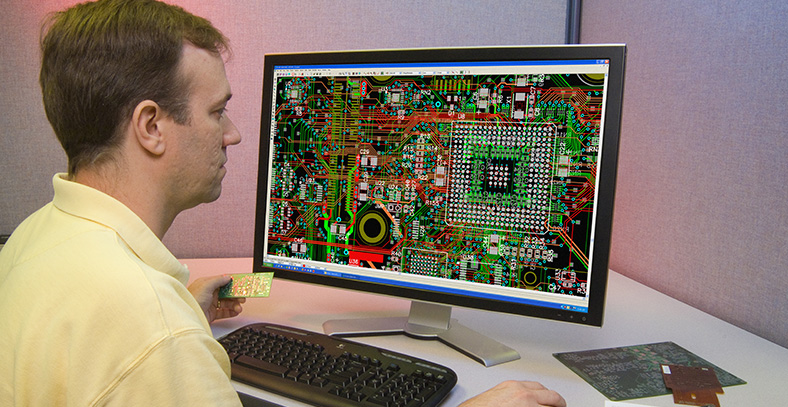
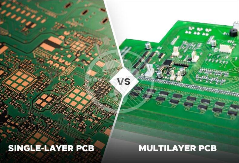
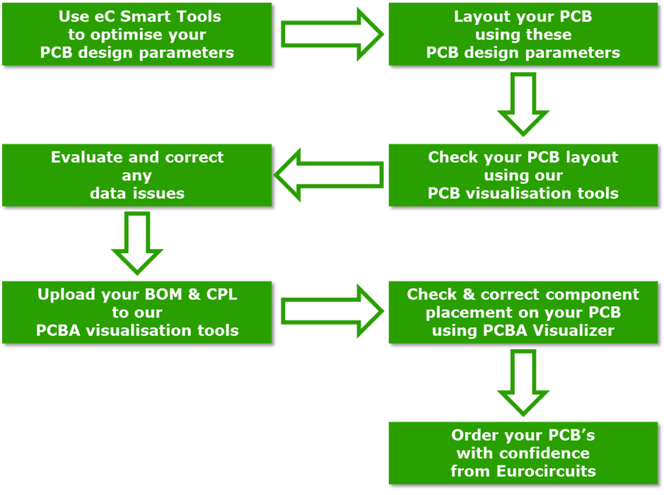
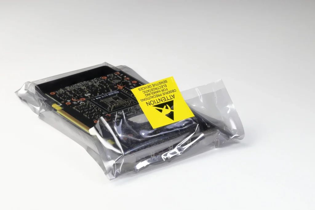
PCB manufacturing is a complex process that begins with PCB design. Designers use a program like Extended Gerber to create the layout. The software encodes the required information, including component symbols and copper trace layers. The PCB design is then forwarded to the manufacturing company. After a DMF check, the PCB schematic is printed on film using a plotter. The film is then used for PCB imaging. Once the film is ready, the manufacturer prepares to manufacture the actual PCB containing the laminate. this is the body that will receive the copper that makes up the PCB.
The next thing to do is to place a layer of photosensitive films called photoresists, which are simply reactive chemicals that harden when exposed to UV light. The film is pinned to the laminate and held in place. An alkaline solution is then used to remove all unwanted copper. Another solvent is then used to wash away the hardened resist used to protect the copper. The layers are then aligned by punching holes using an optical hole punch. The formed layers are then fused together and covered with thin copper foil before they are sandwiched together. Holes are then drilled in the board. These holes will be used for copper connections. They are small holes about 100 microns in diameter.
After drilling, plating is performed to fuse the different layers together, which is done by using chemical deposition. Then a layer of photoresist is applied to the panel. The board is then run through an oven to cure the solder resist. It is then chemically plated with gold and silver plating before being electrically tested to confirm its functionality.
