Printed circuit boards (PCBs) form the basis of all major electronic devices. These marvelous inventions are found in almost all computing electronics, including simpler devices such as digital clocks, calculators, and so on. For those of you who don’t know, PCBs transmit electrical signals through electronic devices, thus fulfilling the electrical and mechanical circuit requirements of the device. In short, PCBs tell where the power goes to bring electronic devices into your life.
PCBs direct current around their surface through a network of copper pathways. The complex system of copper traces defines the unique role of each printed circuit board.
Before proceeding with a PCB design, it is recommended that circuit designers visit a PC board shop and meet face-to-face with the manufacturer regarding PCB manufacturing requirements. It helps prevent designers from passing on any unnecessary errors during the design phase. However, this is becoming impractical as more and more companies outsource their PCB manufacturing consulting to overseas suppliers. Therefore, we are providing this article to have a proper understanding of PCB manufacturing steps. Hopefully, it will give circuit designers and novices in the PCB industry a clear understanding of how printed circuit boards are manufactured and avoid making unnecessary mistakes.
PCB manufacturing process steps
Step 1: Design and Output
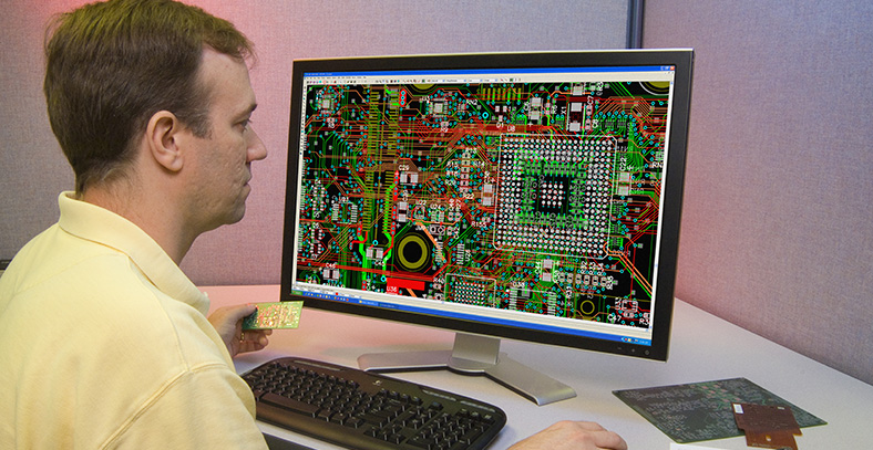
The board should be strictly compatible with the PCB layout created by the designer using PCB design software. Common PCB design software includes Altium Designer, OrCAD, Pads, KiCad, Eagle, etc. Note: Before PCB manufacturing, designers should inform the contract manufacturer of the version of the PCB design software they are using to design the circuit, as it can avoid problems due to discrepancies.
Once a PCB design is approved for production, the designer can export the design to a format supported by the manufacturer. The most common procedure is called extensions to individual files.
The PCB industry has spawned the expansion of the individual file as the perfect output format. Different PCB design software may require different steps of individual file generation, and they all encode comprehensive and important information, including copper trace layers, drill diagrams, holes, component symbols, and other options. At this point, all aspects of the PCB design are checked. The software performs supervisory algorithms on the design to ensure that no errors are found. The designer also checks the plans for elements related to trace width, board edge spacing, trace and hole spacing, and hole dimensions.
After thorough inspection, designers forward the PCB files to the PCB Fab House for production. To ensure that the design meets the minimum tolerances required for manufacturing, almost all PCB Fab Houses are subjected to Design for Manufacturing (DFM) checks prior to board manufacturing.
Step 2: From file to development
PCB printing begins after the designer has output the PCB schematic file and the manufacturer has performed a DFM check. The manufacturer uses a special printer called a plotter to make photographic film of the PCB to print the board. The manufacturer will use these films to image the PCB. Although it is a laser printer, it is not a standard laser printer. The plotter uses incredibly accurate printing technology to provide highly detailed film of the PCB design.
The final product will be a plastic sheet with black ink on the negative side of the PCB. For the inner layer of the PCB, the black ink represents the conductive copper part of the PCB. The rest of the clear part of the image represents the area of non-conductive material. The outer layer follows the opposite pattern: the copper layer is removed, but the black color refers to the area that will be etched away. The plotter automatically develops the film and stores the film securely to prevent unwanted contact.
Each layer of the PCB and solder mask has its own sheet of transparent black film. A total of four sheets are required for a two-layer PCB: two for the multilayers and two for the solder resists. It is important that all the developing shadows must correspond perfectly to each other. When used harmoniously, they can be drawn to create a PCB alignment diagram.
To achieve perfect alignment of all films, alignment holes should be punched in all films. The accuracy of the holes can be determined by adjusting the table on which the film is located. Holes are punched when a slight alignment of the table results in the best match. These holes will be fitted with locating pins in the next step of the imaging process.
