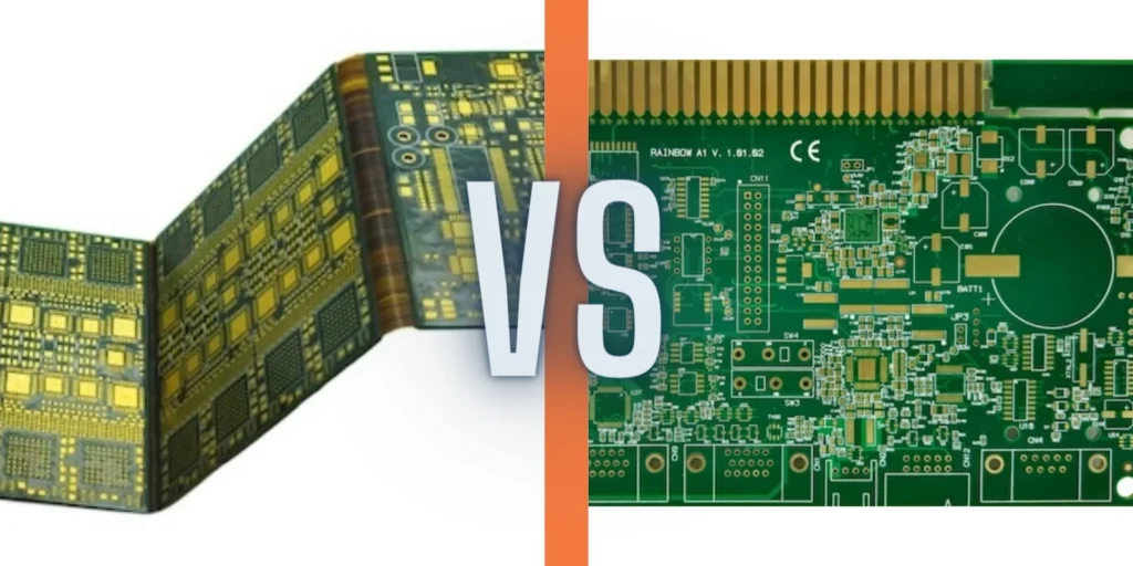
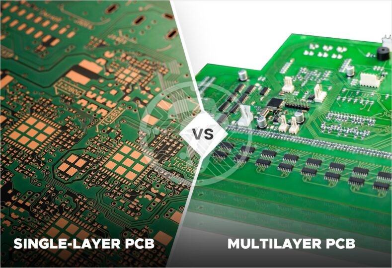
PCB stack design is an important step before circuit board layout design, which involves the arrangement of copper and insulation layers that make up the PCB. Through reasonable stack design, the performance, reliability, and cost of the circuit board can be ensured to achieve the best balance.

1、 Basic principles of PCB stack design
Determine the number and type of layers: Determine the required number of layers based on factors such as the size of the circuit board, component density, signal integrity requirements, electromagnetic compatibility requirements, and component heat dissipation requirements.
Layer arrangement: provides a shielding layer for the device and a reflow plane for the top-level wiring, reducing crosstalk between signals.
Avoid unnecessary impedance and loops: The signal layer and ground layer should be layered adjacent to each other to prevent the generation of RF energy loops.
Symmetry: For multi-layer PCBs, the stacked structure should maintain symmetry as much as possible to reduce warping issues during heating.
2、 Specific stacking design scheme
Four layer laminate scheme: The common four layer laminate scheme is S-G-P-S, where G represents the ground plane, P represents the power plane, and S represents the signal layer.
Another common four layer board scheme is S-G-S-P.
Six layer laminate scheme: Common laminate schemes for six layer laminates include S-G-S-P-G-S and S-S-G-P-S-S.
When choosing a six layer laminate scheme, comprehensive consideration should be given to specific circuit design requirements, signal integrity requirements, EMC requirements, and other factors.
3、 Design considerations
Impedance control: Impedance matching is a fundamental requirement in CB stack design.
In the design process, it is necessary to comprehensively consider the influence of factors such as routing type, dielectric thickness, line width, line spacing, and dielectric material on impedance.
Signal integrity: In PCB design, special attention should be paid to signal integrity issues.
By implementing reasonable stacking design and wiring strategies, issues such as signal reflection, distortion, and loss can be reduced.
Attention to electromagnetic compatibility: Carefully designed stacked structures can minimize electromagnetic radiation and prevent circuits from being affected by external noise sources.
Meanwhile, it can also reduce issues such as signal crosstalk and impedance mismatch.
Cost considerations: When designing PCB stacks, cost factors also need to be taken into account.
On the premise of meeting performance requirements, efforts should be made to minimize the number of layers and material costs.
