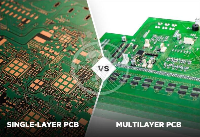
As the core component of electronic devices, the manufacturing process of circuit boards involves multiple precision machining steps.
These links not only determine the performance and quality of the circuit board, but also directly affect the reliability and stability of the final electronic product.
In circuit board manufacturing, precision machining technology is first reflected in the design process.
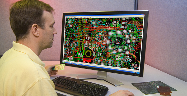
By using advanced design software such as Altium Designer, Cadence Allegro, etc., it is possible to achieve layout and routing at the micrometer level.
Designers need to consider key factors such as line width and spacing, pad size, via size, and positional accuracy to ensure electrical performance and signal integrity.
The precision of this step lays a solid foundation for subsequent processing.

Entering the manufacturing stage, precision machining technology is mainly reflected in the following aspects:
1、 Graphic transfer
Graphic transfer is a crucial step in transferring design patterns onto copper foil layers.
Traditional methods such as photographic plate making have gradually been replaced by laser direct imaging (DI) technology.
DI technology uses high-precision laser to directly draw circuit patterns on copper-clad laminates, reducing the accumulation of errors in traditional processes and significantly improving positioning accuracy and repeatability.
2、 Etching control
Etching is the core step in forming circuit patterns.
By using precise chemical etching or electroplating etching processes, and strictly monitoring process parameters such as etching solution concentration, temperature, time, etc., the consistency and repeatability of line width and spacing can be effectively controlled.
The advanced etching rate monitoring system further ensures the accuracy of the etching process.
3、 Drilling and Electroplating
Drilling is used to create through holes that connect different layers of circuit boards.
By using high-precision CNC drilling machines and combining them with laser drilling technology, precise machining of small apertures can be achieved.
Electroplating is used to deposit a metal layer on the hole wall, ensuring good conductivity and mechanical strength.
The accuracy of this step is equally crucial as it directly affects the electrical connection performance of the circuit board.
4、 Testing and Quality Control
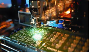
In the production process of circuit boards, advanced detection methods such as automatic optical inspection (AOI) and X-ray inspection (XRAY) are introduced to detect and correct deviations in a timely manner at various key nodes.
These precision inspection equipment can capture tiny defects and ensure that the processing accuracy of the circuit board meets the design requirements.
The precision machining technology in circuit board manufacturing covers multiple aspects such as design, pattern transfer, etching control, drilling and electroplating, as well as inspection and quality control.
The continuous development and optimization of these technologies not only improve the performance and quality of circuit boards, but also promote the development of electronic products towards miniaturization and higher performance.
