PCB wiring is an important step in the design and manufacturing of electronic devices. Different PCB wiring methods have their unique advantages and applicable scenarios. Designers need to choose the appropriate wiring method based on the functional requirements, operating frequency, and design specifications of the circuit.
PCB designers often use special wiring methods that not only improve circuit performance, but also ensure signal integrity and reduce noise interference, thereby ensuring the stability and reliability of electronic products.
Here are several wiring methods:
1. Differential signal wiring
Differential signal wiring is used to transmit high-frequency signals, especially in high-speed digital circuits.
Differential signals have two signal lines, whose voltage values are symmetrical to each other, and the signals are transmitted through two lines, reducing noise and electromagnetic interference.
2. Blind hole and buried hole technology
Blind holes and buried holes are techniques used to increase the number of layers, reduce size, and lower costs of PCB boards.
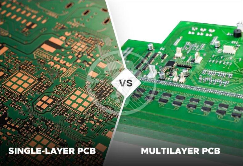
This technology is common in multi-layer PCB design, which can save space and reduce board thickness while maintaining high performance.
3. Microstrip and Strip Lines
Microstrip and strip lines are commonly used for high-speed signal transmission, especially in radio frequency (RF) circuits.
4. Vias type
In PCB design, there are various types of through holes used to achieve electrical connections.
The common types are:
Through holes: penetrate the entire PCB layer and connect the upper and lower layers.
Blind via: Only penetrates from the outer layer to a certain layer of the inner layer.
Buried via: Exists in the inner layer and does not connect to the outer layer.
Microvia: Used for high-density interconnect (HDI) boards, typically used to connect the innermost and outermost layers of a PCB.
5. Power and ground plane wiring
The design of power and ground plane wiring is crucial in high-frequency and high-power circuits.
By designing the power supply and ground layer as continuous large panels, electrical noise and signal interference can be reduced, and power integrity can be improved.
6. Stripe wiring
Interlocking wiring is a wiring method used for signal transmission inside circuit boards.
Its signal line is sandwiched between two ground planes, providing better signal integrity and lower electromagnetic interference (EMI).
7. Interference management
Crosstalk refers to the interference between signal lines on a circuit board.
To reduce crosstalk, the following techniques can be used:
Minimize signal line crossing: Reduce the crossing between signal lines to avoid mutual interference between them.
Appropriate shielding: Add a layer or power layer around the high-frequency signal line as a shielding layer.
Maintain signal line spacing: Increase the spacing between signal lines to reduce coupling between signals.
8. Impedance matching
In high-speed PCB design, impedance matching is used to ensure the quality of signal transmission and avoid signal reflection.
Impedance matching is usually achieved by adjusting the width and spacing of signal lines, as well as using appropriate materials.
