In the manufacturing process of PCB, PCB schematic and PCB design files are two crucial links.Although they are all related to PCB, there are significant differences in definition, content, function, and usage stages.
PCB schematic, also known as circuit schematic, is a diagram that describes the connection relationship between various components in a circuit.
It does not consider the actual physical size and location of components, but only focuses on the logical relationship and electrical performance of the circuit.
In the schematic, we can clearly see the component symbols, connection lines, and network labels in the circuit.
Component symbols represent various components in a circuit, such as resistors, capacitors, inductors, diodes, transistors, etc.
Connection lines represent the electrical connections between various components, while network labels are used to identify the same connection points in the circuit.
This simple two-dimensional circuit design provides engineers with a foundation for understanding the working principles and performance of circuits.
Compared to schematics, PCB design files focus more on actual physical implementation.
It is a detailed graphic and data file used to guide PCB manufacturing and assembly.
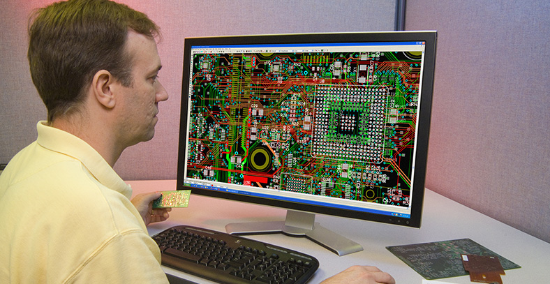
The design document contains actual physical dimensions, positions, wiring, and other information of the components.
In the file, we can see elements such as component packaging, wiring layers, solder pads, vias, silk screen layers, etc.
Component packaging represents the external dimensions and pin layout of actual components, the wiring layer describes the direction and width of wires on the circuit board, solder pads are the connection points between component pins and circuit board wires, and vias are used to achieve electrical connections between different wiring layers.
The silk screen layer is used to label the names, symbols, and other information of components on the circuit board, to help engineers identify and locate them more conveniently during assembly and use.
In terms of functionality, PCB schematics are mainly used for circuit analysis and design.
It is one of the earliest documents formed in the development process of electronic products, providing a foundation for subsequent PCB design.
Through schematics, engineers can clearly understand the logical relationships and electrical performance of circuits, enabling them to modify and optimize them.
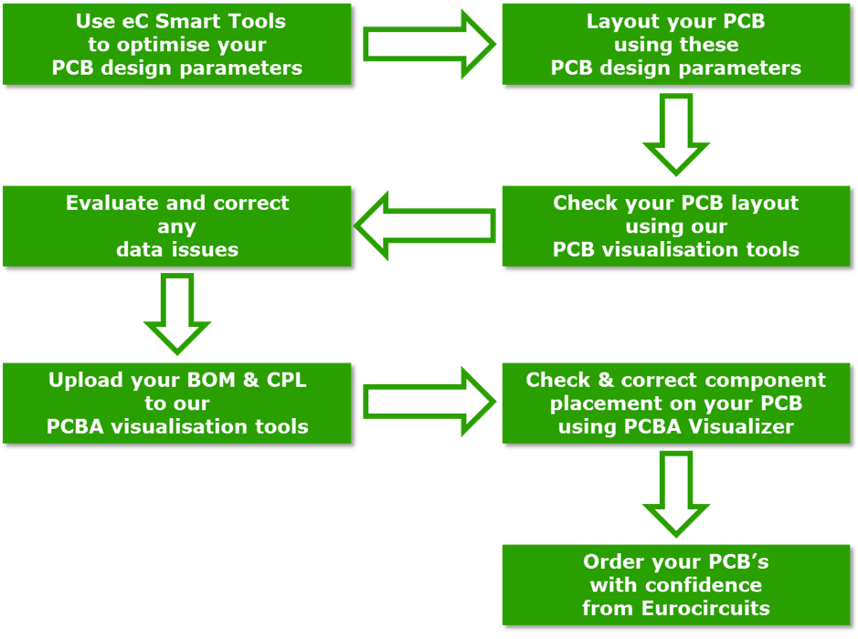
PCB design files are mainly used to guide the manufacturing and assembly process of PCBs.
It is a crucial step in transforming schematics into actual circuit boards, directly determining the performance and reliability of electronic products.
During the manufacturing process, the manufacturer will design the layout and wiring of components according to the requirements of the design documents to ensure that the circuit board can meet the expected performance requirements.
In addition, there are differences between PCB schematics and PCB design files in terms of user groups and usage stages.
Schematics are mainly used by electronic engineers, designers, and maintenance personnel for circuit analysis, modification, and optimization in the early stages of the design process.
And design files are more commonly used by PCB manufacturers and assembly factories to implement the physical layout and wiring of circuits after the schematic is verified and optimized.
Overall, PCB schematics and PCB design files each play different roles in electronic engineering.
They complement each other and together constitute the entire process of electronic devices from design to production.
Understanding and mastering the differences between them is crucial for electronic engineers.
Only by deeply understanding the characteristics and functions of these two links can we better carry out circuit design and optimization, providing strong guarantees for the performance and reliability of electronic devices.
