There are differences in position, function, manufacturing, and cost between the inner and outer layers of PCB. The inner layer is responsible for electrical connections, which is complex and costly to manufacture; The outer layer is connected to the outside world, with simple manufacturing and low cost, but it needs to consider aesthetics and wear resistance.
1、 Differences in location and structure
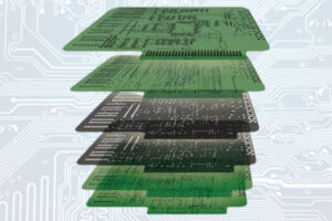
The inner layer of a PCB is located between the top and bottom layers and is an important component of a multi-layer PCB, mainly used for signal transmission and power distribution. The inner layer board is mainly composed of alternating conductive and insulating layers. The design of the inner layer requires precise control of the width, spacing, and interlayer connections of the conductive paths to ensure signal integrity and power stability.
The outer layer board, namely the top and bottom layers, is the outermost layer of the PCB. The conductive paths and component layout on the outer layer board are more complex. The top layer is used to place components, while the bottom layer is mainly used for wiring and soldering. In addition to considering electrical connections, the design of the outer panel also needs to take into account wear resistance, chemical corrosion resistance, and aesthetics.
2、 Differences in functionality and usage
The inner board is mainly used to achieve electrical connections inside the PCB, carrying key circuits such as power, signal, and ground wires
In addition to achieving electrical connections, the outer board also undertakes the task of connecting with external interfaces. The top and bottom layers are covered with soldering points for connectors, switches, indicator lights, and other components. In addition, the silk screen layer on the outer board is used to label the projection outline, label, nominal value, or model information of the components.
3、 Manufacturing and process differences
The manufacturing process of the inner layer board is relatively complex, involving multiple steps such as lamination, drilling, and electroplating of multi-layer boards. It is necessary to strictly control the thickness of the conductive layer, the uniformity of the insulation layer, and the alignment accuracy between layers, and also consider the alkali and heat resistance of the material.
The manufacturing process of the outer layer board is relatively simple, mainly involving the treatment of insulating substrates, deposition of conductive layers, and formation of patterns. The conductive paths and component layouts on the outer board are usually formed by screen printing, photolithography, or directly depositing conductive materials on insulating substrates. In order to improve wear resistance, corrosion resistance, and aesthetics, a protective layer (such as a solder mask) will also be covered on the outer board.
4、 Cost and Considerations
Due to the complex manufacturing process and high requirements for materials and environment of the inner layer board, its cost is usually high. When designing the inner panel, it is necessary to balance factors such as electrical performance, manufacturing cost, and reliability.
The manufacturing cost of outer panels is relatively low, but additional factors such as aesthetics, wear resistance, and corrosion resistance also need to be considered. In the design and manufacturing process of outer panels, attention should also be paid to details and quality control.
