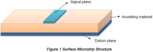
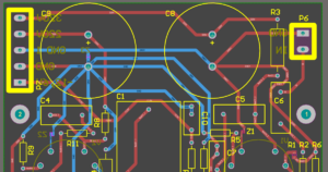
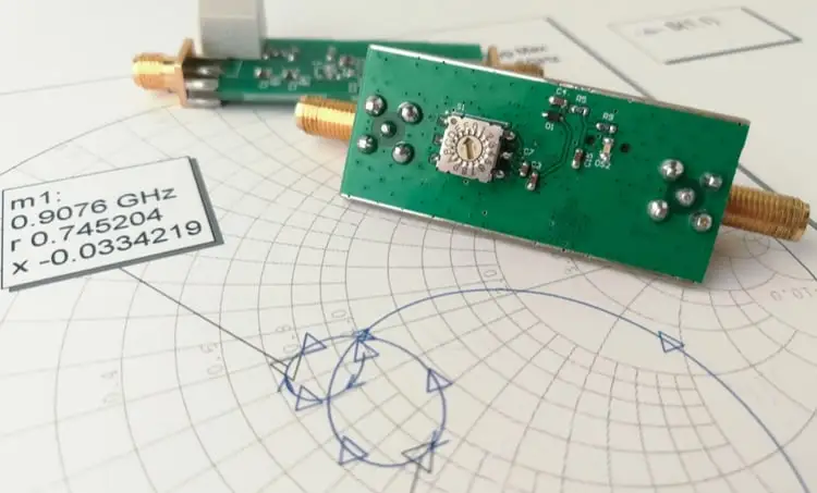
In general, the following factors affect the characteristic impedance of a PCB: dielectric thickness H, copper thickness T, width of the alignment W, spacing of the alignment, dielectric constant Er of the material selected for the stack, and thickness of the solder resist.
In general, the higher the dielectric thickness and line spacing the higher the impedance value; the higher the dielectric constant, copper thickness, line width, and solder resist thickness the lower the impedance value. The relationship between these factors and the characteristic impedance is shown in the figure below.
First: dielectric thickness, increasing dielectric thickness can increase impedance and decreasing dielectric thickness can decrease impedance; different semi-cured sheets have different adhesive content and thickness. Its thickness after pressing together is related to the flatness of the press and the procedure of pressing the sheet; for any kind of sheet used, it is necessary to obtain the thickness of the media layer it can produce to facilitate design calculations, and engineering design, press control, and incoming material tolerance are the keys to media thickness control.
The second: line width. Increasing the line width reduces the impedance and decreasing the line width increases the impedance. Line width control requires within +/-10% tolerance to better achieve impedance control requirements signal line gap affects the entire test waveform, its single point impedance is high, making its entire waveform uneven, impedance line is not allowed to fill the line, the gap can not exceed 10%. Line width is mainly controlled by etching control. In order to ensure the line width, according to the etching side etching amount, light drawing error, graphic transfer error, the engineering negative for process compensation to achieve the line width requirements.
Third: copper thickness, reduce the line thickness to increase impedance, increase the line thickness to reduce impedance; line thickness can be controlled by graphic plating or by selecting the appropriate thickness of the base material copper foil. The control of copper thickness requires uniformity, for thin lines, isolated lines of the board plus a shunt block, which balances the current to prevent uneven copper thickness on the line, affecting the impedance of the cs and ss side of the copper distribution is extremely uneven, to cross the board on the board to achieve the purpose of uniform copper thickness on both sides.
Fourth: dielectric constant. Increasing the dielectric constant reduces the impedance and decreasing the dielectric constant increases the impedance, and the dielectric constant is mainly controlled by the material. The dielectric constant varies from sheet to sheet and is related to the resin material used: FR4 sheet has a dielectric constant of 3.9-4.5, which decreases as the frequency increases, and PTFE sheet has a dielectric constant of 2.2-3.9, which requires a high impedance value for high signal transmission and thus a low dielectric constant.
Fifth: Resist thickness, printed resist will reduce the outer impedance. Under normal conditions printing resist once can make the single end drop 2 ohms, can make the differential drop 8 ohms, printing 2 times the drop value is twice as much as when printing once, when printing 3 times or more, the impedance value no longer changes.
