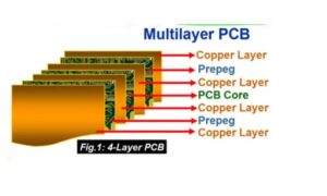
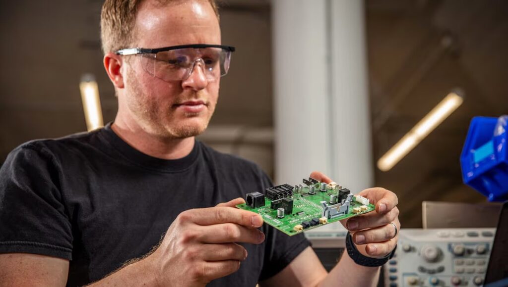
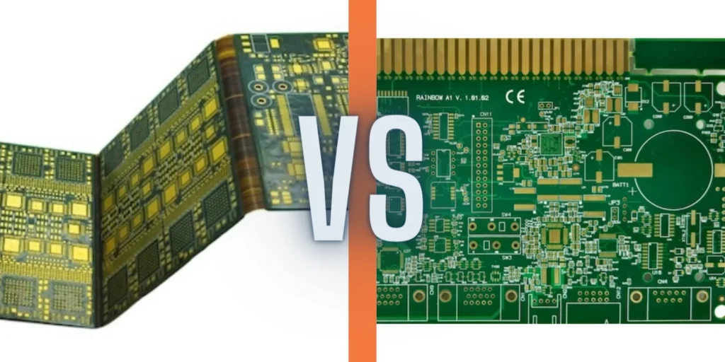
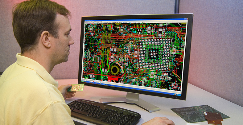
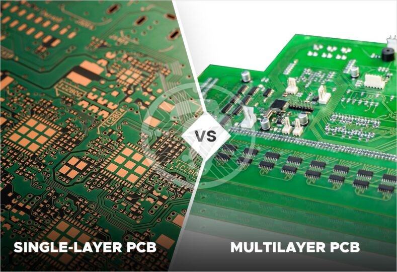
PCB is composed of multiple layers of materials, each layer has its specific function, and each layer cooperates with each other. Each layer has its specific function and importance, together forming a complete electronic circuit.
The following are the main functions of each layer on a PCB circuit board:
1、 Signal Layer
The signal layer is used to transmit electronic signals and is usually made of copper foil, which is etched to form circuit patterns.
The number of signal layers depends on the complexity of the PCB. Simple PCBs may only have one signal layer, while complex PCBs may have multiple signal layers, including top layer, bottom layer, and mid layer. The top and bottom layers can also be used for placing and soldering components.
2、 Power Plan and Ground Plan
The power layer is used to provide power to electronic components on the PCB, while the ground layer is used to provide grounding connections for electronic components.
These two layers are usually made of copper foil and etched to form power or ground circuit patterns, which help reduce power noise and signal interference, improve circuit stability and performance.
3、 Solder Mask Layer
The solder mask layer is used to prevent oxidation and corrosion of circuits on the PCB, as well as to prevent solder from adhering to areas that do not require soldering during the soldering process.
The solder mask layer is usually made of green or other colored solder mask ink, which not only provides protection but also improves the aesthetics and readability of the PCB.
4、 Silkscreen Layer
The silk screen layer is used to identify electronic components and circuits on a PCB, usually made of white or other colored silk screen ink, which can print the outline, labels, and various annotation characters of the components.
5、 Mechanical Layer
The mechanical layer is used to define the external dimensions, cutting slots, assembly positioning marks, and other mechanical processing information of the PCB.
It provides reference information for PCB manufacturing and installation, ensuring the accuracy and consistency of the PCB. The mechanical layer can also output displays together with other layers, but should not be used for electrical wiring.
6、 Prohibit wiring layer (Keep Out Layer)
Prohibited wiring layer is used to define the area on the circuit board where components and wiring can be placed.
By drawing enclosed areas, the wiring layer is prohibited from setting boundaries for automatic layout and routing, ensuring the effectiveness of circuit design.
7、 Other layers
In addition to the above-mentioned layers, PCBs may also contain other layers, such as:
Multi Layer: Used to increase the number of layers in a PCB, improve its integration and performance.
Drill Layer: Provides drilling information during the circuit board manufacturing process, such as the drilling positions of solder pads and vias.
Paste Mask Layer: mainly used for making steel mesh in surface mount technology (SMT).
The holes on the steel mesh match the size of the solder pads, ensuring that the solder paste can be accurately applied to the solder pads.
Impedance Control Layer: Used to specify and control the impedance of signal lines on PCBs to ensure the quality and consistency of signal transmission.
