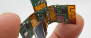
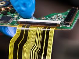
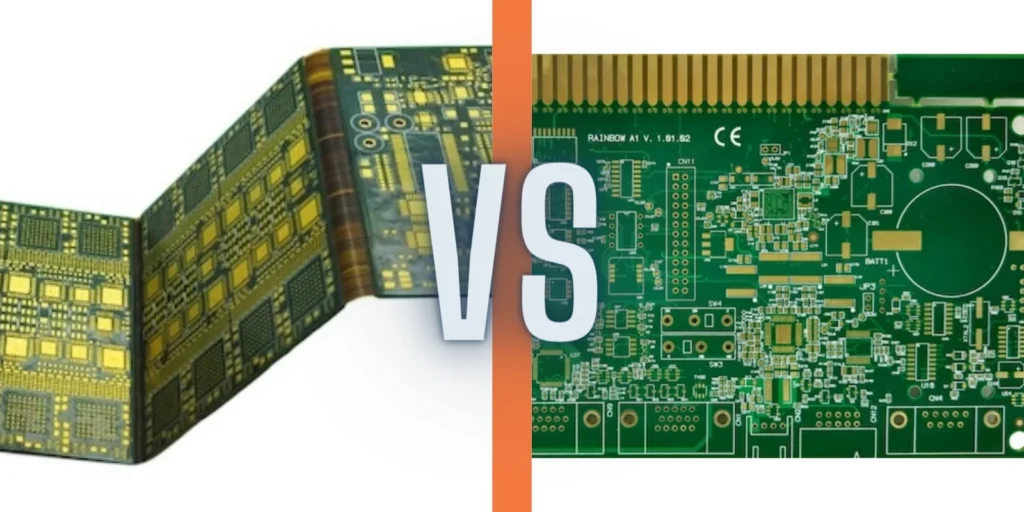
The birth and development of FPC and PCB has given rise to a new product, the flexible and rigid PCB. Rigid and flexible PCBs are flexible boards and rigid boards that have been pressed together through processes such as lamination to form boards with FPC characteristics and PCB characteristics according to the relevant process requirements.
Cutting:Rigid substrate cutting: cutting large areas of copper clad board to the size required by the design.
Softboard substrate uncutting: cut original rolls (substrate, pure adhesive, cover film, PI reinforcement, etc.) to the size required by the engineering design.
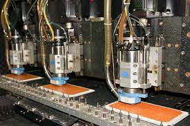
Drill:Drill pilot holes for line connections.
Black hole:Use the potion to make the toner stick to the wall of the hole, which plays a good role in connecting the conductivity.
Copper plating:A layer of copper is plated inside the hole for conduction.
Alignment exposure: aligning the film (negative) under the corresponding hole where the dry film has been applied to ensure that the film graphics can be properly overlapped with the board surface, and the film graphics are transferred to the board surface dry film by the principle of light imaging.
Developing: The dry film in the unexposed areas of the line graphics is developed off by potassium carbonate or sodium carbonate, leaving the dry film graphics in the exposed areas.
Etch:The area of the line graphic that is exposed to the copper surface after development is etched away by an etching solution, leaving the portion of the graphic covered by dry film.
AOI: Automated optical inspection, which is the principle of optical reflection, transmits the image to the device for processing, and compares it with the set information to detect the open and short circuit problems of the line.
Lamination:On copper foil wiring, covered with an upper layer of protective film to avoid oxidation or short circuiting of the wiring, while acting as insulation and product bending.
Cutting:Hardboard substrate cutting: cutting large areas of copper clad board to the size required by the design.
Softboard substrate uncutting: cut original rolls (substrate, pure adhesive, cover film, PI reinforcement, etc.) to the size required by the engineering design.
Drill:Drill pilot holes for line connections.
Black hole:Use the potion to make the toner stick to the wall of the hole, which plays a good role in connecting the conductivity.
Copper plating:A layer of copper is plated inside the hole for conduction.
Alignment exposure: aligning the film (negative) under the corresponding hole where the dry film has been applied to ensure that the film graphics can be properly overlapped with the board surface, and the film graphics are transferred to the board surface dry film by the principle of light imaging.
Developing: The dry film in the unexposed areas of the line graphics is developed off by potassium carbonate or sodium carbonate, leaving the dry film graphics in the exposed areas.
Etch:The area of the line graphic that is exposed to the copper surface after development is etched away by an etching solution, leaving the portion of the graphic covered by dry film.
AOI: Automated optical inspection, which is the principle of optical reflection, transmits the image to the device for processing, and compares it with the set information to detect the open and short circuit problems of the line.
Lamination:On copper foil wiring, covered with an upper layer of protective film to avoid oxidation or short circuiting of the wiring, while acting as insulation and product bending.
Pressing CV: The pre-stacked cover film and the reinforced panels are pressed together as a single unit by high temperature and pressure.
Punching: Using a die, the work plate is punched and cut by mechanical punching power to a shipping size that meets the customer’s production use.
Lamination (soft and rigid board lamination)
Pressing: The soft and hard boards are pressed together by heat pressing under a vacuum that gradually heats up the product.
Secondary drilling: Drill the pilot holes for the connection between the soft and hard boards.
Plasma cleaning:Using plasma to achieve results that cannot be achieved by conventional cleaning methods.
Sunken copper (hard plate):A layer of copper is plated inside the hole for conduction.
Copper plating (hard plate):Using plating to thicken the thickness of the hole copper and face copper.
Line (apply dry film):A layer of photosensitive material is applied to the surface of the sheet that has been copper plated to serve as a film for graphic transfer. Etching AOI linkage:Erodes the desired graphics by dissolving all the copper surface outside of the line graphics.
Solder resist (silkscreen):Covers all wiring and copper surfaces to protect the wiring and insulation.
Solder resist (exposure):The ink undergoes a photopolymerization reaction and the ink in the screen printed area is retained on the board and cured.
Laser uncovering: Using a laser cutter, a specific degree of laser cutting is performed at the location of the hard and soft intersection lines to uncover the hard part of the board and expose the soft part of the board.
Assembly: Apply steel or reinforcement to the corresponding area of the board to provide bonding and increase the hardness of the important parts of the FPC.
Testing:Probe to test if there is any defective open/short circuit to ensure product functionality.
Characters:Marking symbols are printed on the board surface for easy assembly and identification of subsequent products.
Gong plate:Milling the desired shape according to the customer’s requirement by CNC machine.
FQC:Check the appearance of the finished products that have been produced according to the customer’s requirements and pick out the defective products to ensure the quality of the products.
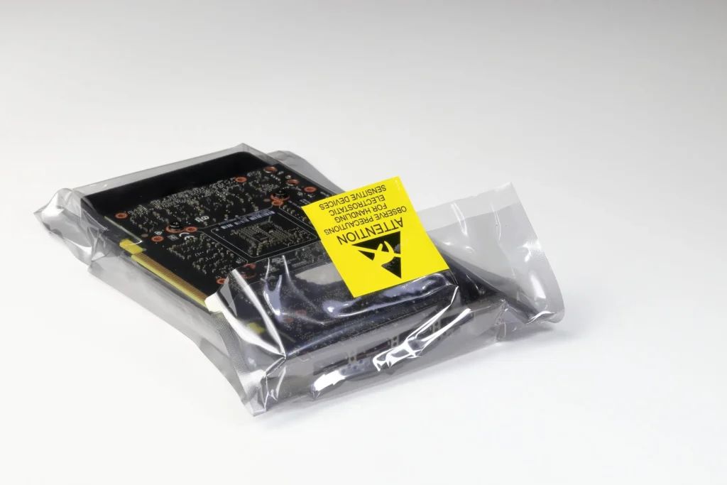
Packaging:The fully inspected Ok boards are packaged according to customer requirements and warehoused for shipment.
