What is a delay circuit? 6 kinds of delay circuit principle explanation – FAST TURN PCB
As we all know, when it comes to delay, many people will think of using software to achieve, such as timers and so on. Today, it is said that the way to achieve timing with hardware, although not so accurate, but some occasions are still used. Today we are going to introduce 6 kinds of delay circuit working principle.
1. Accurate long delay circuit diagram
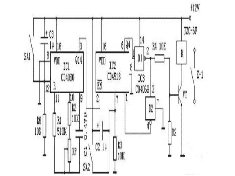
The circuit is composed of CD4060 timer base circuit, timer base pulse generated by the circuit, through the internal part of the frequency divider output time base signal. In the frequency division circuit through the peripheral frequency division, to obtain the required timing control time.
After electrification, the time base oscillator oscillates through frequency division and outputs the time base signal. IC2, acting as a divider, starts counting dividers. When the count reaches 10, Q4 outputs high level, the high level changes to low level through D1 reverse phase to make VT cut off, relay power release, cut off the controlled circuit power supply.
At the same time, D1 output low level is inverted to high level by D2 and then added to CP terminal of IC2, so that the high level of output terminal is maintained.
After the circuit is energized to reset IC1 and IC2, the four output terminals of IC2 are all low level. The low level of Q4 output becomes high level through D1 reverse phase, and MAKES VT conduction through R4, and the relay is energized and absorbed. This working state is switched on and timed off.
2. RC delay circuit

RC delay circuit is shown in the figure. The delay time of the circuit can be adjusted by R or C. However, due to the simplicity of the delay circuit, it has the disadvantages of short delay time and low accuracy. For the need for a long time delay and accurate occasions, should choose the time relay as well.
In automatic control, sometimes in order to control the object in a specified period of time work or make the next operation instruction at the appropriate time, often use relay delay circuit. Figure shows several relay delay circuits.
The circuit shown in Figure (a) is a slow and slow suction circuit. When the circuit is on and off, RC’s charge-discharge action is used to realize the delay of suction and release. This circuit is mainly used in the occasion of short delay suction. Sometimes, according to the need of control, only slow release of relay is required, but slow suction is not allowed. In this case, the circuit as shown in Figure (b) can be used.
When just connected to the power supply, because the contact kK-L is normally open, so the RC delay circuit will not have a delay effect on the suction time, and when the relay K. After suction, its contact KK-1 is closed, so that the release of relay Kk can be carried out slowly. Simply calculate the time delay generated by RC delay circuit, such as R=470K, C= 0.15uF time constant R*C directly on the line.
3, 555 simple long delay circuit
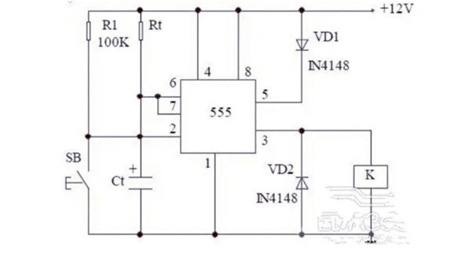
When the button SB is pressed, the 12V power supply charges the capacitor Ct through the resistor Rt, making the potential of pin 6 rise continuously. When the potential of pin 6 rises to the potential of pin 5, the circuit reset time ends.
Because a diode VD1 is attached to the 5-pin string, the 5-pin potential is increased, so it has a longer timing than normal connections (suspended or grounded by a small capacitor).
4. Long delay circuit composed of two 555 time base circuits
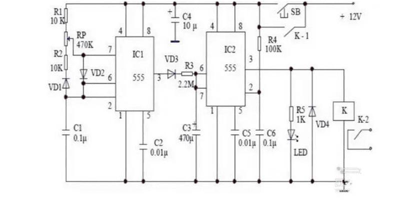
The IC1 555 time-base circuit is connected to a self-excited multivibrator with adjustable duty cycle. When the button SB is pressed, THE DC voltage of 12V is added to the circuit. As the voltage of capacitor C6 cannot be mutated, pin 2 of IC2 circuit is low level, IC2 circuit is in position state, pin 3 outputs high level, relay K is charged, contacts K-1 and K-2 are closed, after k-1 contact is closed, self-locking state is formed. K-2 contact is connected to the electrical equipment to control the on and off of the electrical equipment.
At the same time, the IC1 555 time base circuit starts to oscillate, so the 3 pins alternately output high and low levels. When the 3-pin output is high, charge the capacitor C3 through diode VD3 and resistor R3.
When the 3-pin output is low, diode VD3 cuts off and C3 is not charged. Therefore, C3 is charged only when the 3-pin output is high, so the charging time of capacitor C3 is longer.
When the potential of capacitor C3 rises to 2/3VDD, IC2 555 time-base circuit is reset, 3-pin output low level, relay K loses power, contacts K-1 and K-2 are disconnected and return to the initial state to prepare for the next timing.
5, single operation amplifier composed of single stable delay circuit
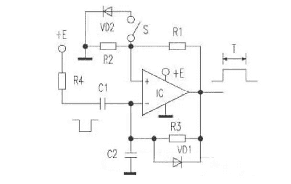
Normally, the IC output remains low and this state is stable. When the negative pulse is input to the inverting end through C1, the potential of the inverting end is lower than that of the in-phase end, and the output end changes from low level to high level. This state is unstable.
This high level is added to the in-phase end of IC after partial pressure of R1 and R2, so that the in-phase end potential is higher than the inverting end, so as to maintain the high level output. At the same time, the high level is charged by R3 and C2. When the voltage on C2 is charged so that the potential of the inverting end is higher than that of the in-phase end, its output end is flipped to the low level again.
At this point, the in-phase potential is about zero, and the voltage on C2 rapidly discharges to the output through VD1, accelerating the circuit back to its initial state.
After the circuit is stabilized, the potential of the inverting end is still higher than that of the in-phase end, so that the output low level can be maintained.
The delay time T of the circuit depends not only on R3 and C2, but also on the partial voltage ratio of R1 and R2.
Therefore, it is very convenient to adjust the delay time. C2 and R3 can be adjusted for coarse delay adjustment, and R2 can be adjusted for fine delay adjustment (if the partial pressure ratio is 1/2 to 2/3, the delay accuracy is higher).
However, the state of the circuit is random when it is powered on. To make the circuit have a unique output state after it is powered on, there are two methods:
First, add R4 to the circuit. In this way, when powering on, since the voltage on C1 cannot be abrupt, the power supply voltage can be put in low level by adding R4 and C1 to the inverting end;
The other is a diode VD2 and a switch S(as shown by the dotted line) at the in-phase end to the ground.
If the output is high level during power-on, although this state is unstable, as mentioned above, it will take time T before the output becomes low level, and in practice, it often requires immediate reset during power on the circuit.
Therefore, S can be switched on first when powering on. If the output is high level, C2 can be charged to 0.7V to reset the circuit, greatly shortening the time of electrical reset on the circuit. After reset, disconnect S, and the circuit can work normally.
6, transistor delay circuit
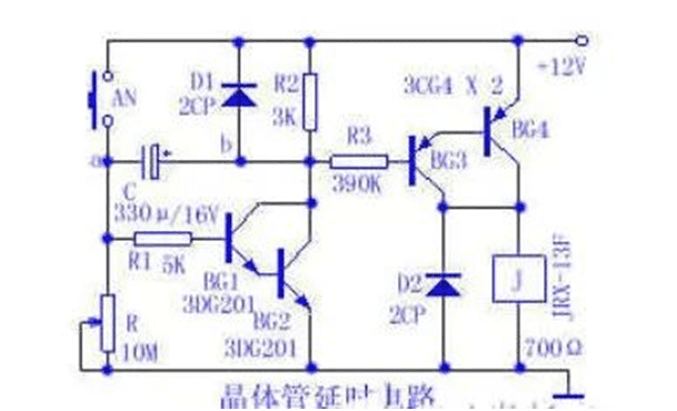
The delay part consists of a Miller integral circuit composed of BG1 and BG2 and capacitor C. The terminal voltage of C is zero before the power supply is connected. After the power supply is connected, BG3 and BG4 are turned on, and the relay J is closed. At the same time, the capacitor C is charged, and the charging electricity flows through R2, C and R to form a loop.
The potential of a and B compensate each other, so that the potential rise of point A is very small, and the charging current is nearly constant.
When the potential of point B rises to about 10V, BG3 and BG4 approach cut-off, relay J is released, and the delay process ends. Press the button AN, capacitor C rapidly discharges through D1, relay J pulls in, and the next delay process begins.
Delay circuit is often used, RC circuit is relatively simple circuit. Of course, changing the parameters of each component of the circuit can achieve different delays.
We offer professional design solutions covering all aspects of PCB and PCBA layout, including the following board technologies.
Include:
1.PCB design: free laminated design and impedance calculation.
2.PCB manufacturing :PCB board making capacity of 1-48 layers, blind hole, copper thickness up to 12 ounces
3. Component purchase :BOM purchase within 3 days
4.PCB assembly: urgent sample and batch assembly processing, only 1-3 days
5. Functional testing
6. Electronic assembly global logistics
7. Single, double-sided, multi-layer board
8. Rigid circuits, flexible circuits and rigid-flexible circuits.
Please email us to get a quote right away: sales@fastturnpcbs.com
Telephone number: 15018735409
