You may have heard of blind buried-hole boards a lot in the printed circuit board manufacturing industry. To better understand blind buried vias, please continue reading about blind buried hole PCBs below.
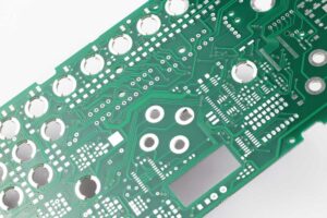
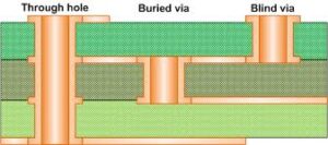
Blind and buried vias are typically used to make connections between PCB layers where space is at a premium. Blind vias connect the outer layer to one or more inner layers, but not through the entire board. Buried vias connect two or more inner layers, but not through the outer layer.
What is a blind hole?
Blind holes are connected from the inner to the outer layer and do not penetrate the entire board.
What is a buried hole?
The buried vias are connected between the inner layers and are not visible from the surface of the PCB.
What are vias? Through-holes are copper-plated holes in printed circuit boards that can be used for connections between layers. The standard through-hole is called a vias, but there are several disadvantages to using vias in surface mount technology (SMT). Therefore, we often use blind or buried vias. Blind or buried vias can be handled in many different ways, including inserting copper buried film vias, inserting soldermask vias, plating vias, or interleaving vias.
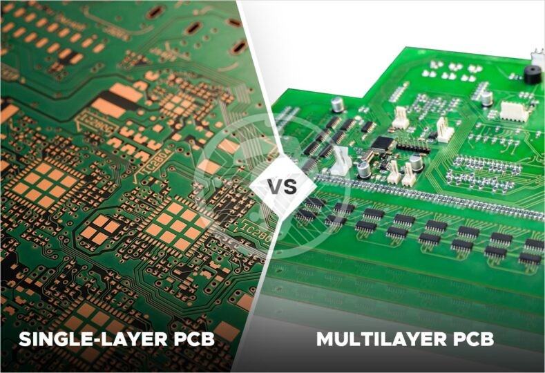
Guangzhou Jujin Technology has many years of experience in manufacturing printed circuit boards with blind and buried vias. No matter what happens, we will complete the process of blind and buried holes to meet the functional requirements of the PCB according to your specific requirements. In addition, we also specialize in making difficult PCB circuit boards, high frequency PCB circuit boards, multi-layer PCB circuit boards, and more.
