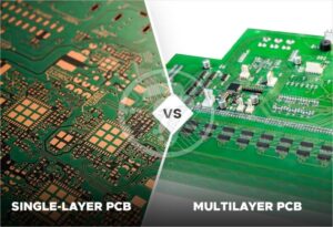
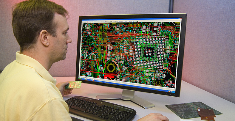
The increased concentration of IC packages leads to higher concentration of interconnects, which requires the use of multiple substrates. Unpredictable design issues such as noise, stray capacitance, crosstalk, etc. can occur in the layout of printed circuit boards. Therefore, printed circuit board design must focus on minimizing signal line length and avoiding parallel paths. Obviously, these requirements cannot be satisfactorily met in a single panel, or even in a dual panel, due to the limited number of crossovers that can be achieved. In the case of a large number of interconnections and crossover requirements, in order to obtain satisfactory performance, the board must be extended beyond two layers, thus forming a multilayer board. Thus, the original purpose of manufacturing multilayer boards was to provide greater freedom in selecting appropriate wiring paths for complex and/or noise-sensitive electronic circuits.
Multi-layer PCBs are as the name implies. Two or more layers of boards can be called multilayers, such as four, six, eight, etc. Of course, certain designs are three- or five-layer circuit boards and are also referred to as multilayer PCBs. The conductive alignment diagram is larger than a two-layer board. The layer is separated from the layer by an insulating backing. After each layer is printed, the layers are overlapped by pressing. After drilling holes, the conductivity between the layers of the line is achieved using through holes. So what are the advantages of multilayer PCB boards? The multilayer PCB board manufacturer will tell you next.
The advantage of multilayer PCBs is that the circuitry can be distributed over multiple layers of wiring, allowing more complex products to be designed. Or smaller products can be made to function with multilayer boards. For example, cell phone boards, pico projectors, recorders, and other volume products. Additional layers provide greater design flexibility, better control over differential and single-ended impedance, and better output at certain signal frequencies.
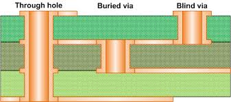
Multi-layer circuit boards are the natural result of the evolution of high speed, multi-functional, high capacity, and small form factor electronics. With the continuous development of electronic technology, especially the widespread use of large-scale and super-large-scale integrated circuits, multilayer printed circuitry is rapidly advancing towards higher density, higher precision, and higher level of digitization. And high precision lines, micro small holes, blind holes, buried holes, thick copper plate and other technologies can meet market demand. Due to the demand for high-speed circuits in the computer and aerospace industries. Further increase in packaging density, coupled with the reduction in the size of discrete components and the rapid development of microelectronics technology, the direction of size and mass reduction of electronic devices is shrinking. Due to the limited space available, it is not possible to use single- and double-sided printed boards. Further improvements in assembly density were achieved. Therefore, it was necessary to consider the use of more printed circuits than double layers. This created the conditions for the emergence of multilayer boards.
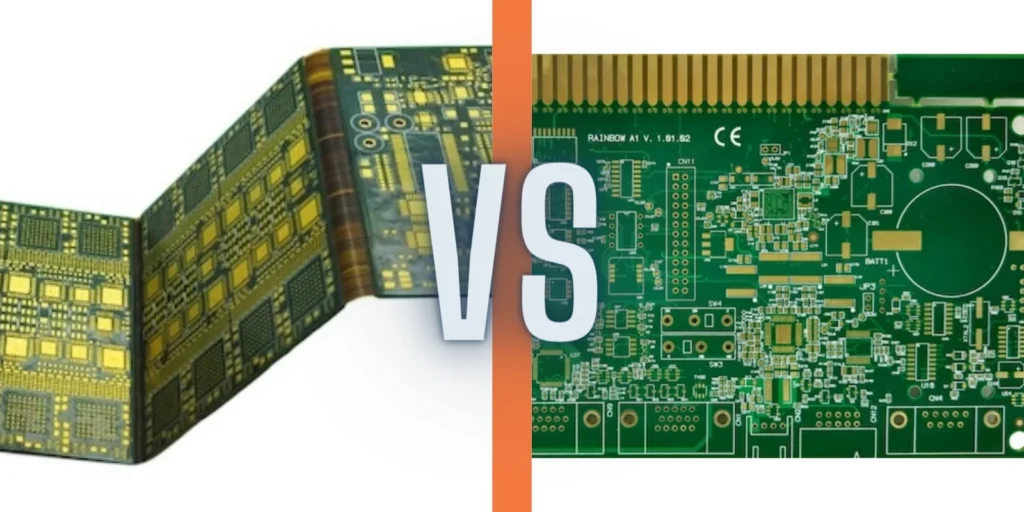
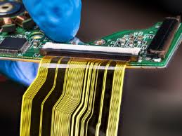
These are the analysis and summary of the PCB suppliers. Of course, multi-layer circuit boards may not be mentioned in this article. Customers are welcome to add to it. We also welcome customers from all over the country to visit our company. We can provide you with high quality double-sided PCB design, PCB prototyping and PCB small to medium volume service. In addition, we also offer PCB rigid-flex PCB manufacturing services and SMT placement services.
