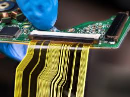
The key to PCB welding quality inspection includes visual inspection, electrical testing, X-ray testing, automatic optical testing, and environmental adaptability testing. These methods ensure welding quality and improve the stability and reliability of electronic equipment.
1、 Visual inspection
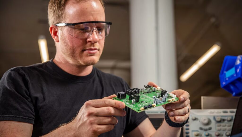
Firstly, the most intuitive and commonly used detection method is visual inspection. Carefully observe the solder joints with the naked eye or microscope to check the shape, gloss, and integrity of the solder. A good welding point should present a smooth, uniform, and complete solder coverage, without obvious burns, voids, or solder joints. In addition, it is necessary to check whether the components are installed correctly, whether there is any damage or tilting, and whether there are impurities or residues around the welding points.
2、 Electrical testing
Electrical testing is an important means of evaluating the quality of PCB welding. By using professional testing equipment such as a multimeter, oscilloscope, etc., electrical parameters such as voltage, current, and impedance are measured at various solder joints on the PCB. These tests can reveal whether there are poor electrical connections, short circuits, or open circuits at the welding points. At the same time, functional testing can also be conducted on the entire PCB to verify whether its overall electrical performance meets the design requirements.
3、 X-ray testing
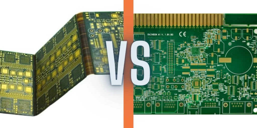
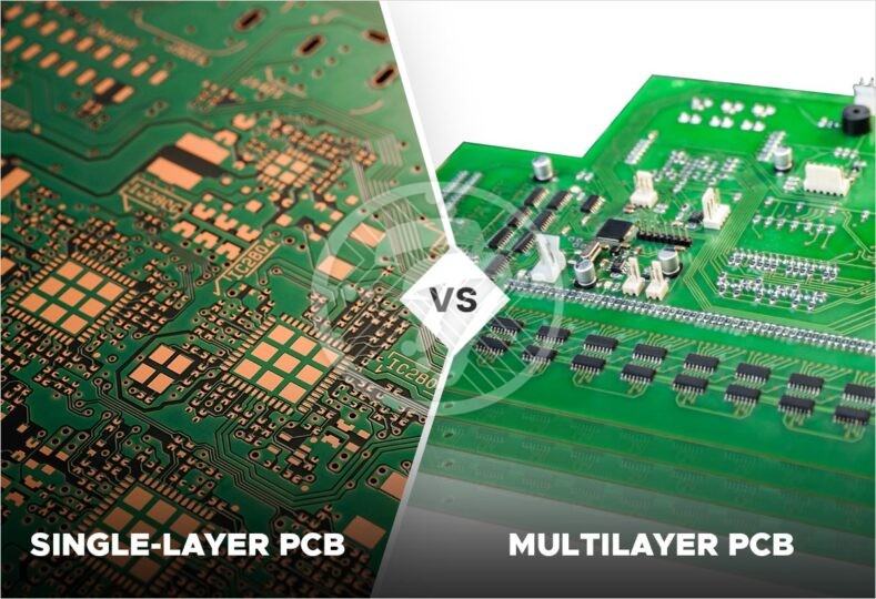
For multi-layer or high-density PCBs, X-ray testing has become an effective quality inspection method. X-rays can penetrate various layers of a PCB, displaying the structure and quality of internal solder joints. By using X-ray images, it is possible to detect voids, cracks, or other potential defects inside the welding point, which may not be detected by conventional visual inspection.
4、 Automatic Optical Inspection (AOI)
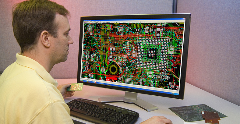
With the development of technology, Automatic Optical Inspection (AOI) systems play an increasingly important role in PCB welding quality inspection. The AOI system captures PCB images through high-resolution cameras and uses advanced image processing algorithms for automatic analysis and recognition. It can quickly detect issues such as missing, misaligned, and poor welding of solder joints, and provide detailed inspection reports. The AOI system not only improves detection efficiency, but also greatly reduces the possibility of human errors.
5、 Environmental adaptability testing
To ensure that PCBs can function properly under various environmental conditions, environmental adaptability testing is also an essential part. This includes temperature cycling testing, humidity and heat testing, vibration testing, etc. Through these tests, the stability and reliability of PCB solder joints in different environments can be evaluated, ensuring that the product can function properly under various harsh conditions.


