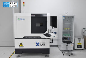
The principle of X-ray detection of PCBA is to use X-ray to irradiate the sample, and then convert the difference in X-ray transmission intensity into a grayscale contrast image through an image receiving conversion device. In this way, different materials will present different grayscale values on the image, allowing for clear observation of the internal structure and possible defects of PCBA, which can be used for the detection of the following items.
1. Material identification and classification: Through X-ray testing, various materials on PCBA can be clearly identified, such as solder joints, metal packaging shells, etc., and classified based on their material density and thickness. This is crucial for subsequent quality control and troubleshooting.
2. Defect detection: X-rays can penetrate the surface of PCBA and discover internal defects such as voids and cracks. These defects are difficult to detect during routine visual inspections, but may have a serious impact on the performance and safety of electronic devices. Through X-ray testing, these potential issues can be identified at an early stage, thereby improving product quality.
3. Evaluation of welding quality: Welding is a key link in the PCBA manufacturing process. X-ray inspection can clearly display the shape and internal structure of the solder joint, helping to evaluate the welding quality. For example, by detecting, it is possible to detect defects such as bubbles and lack of fusion in solder joints, which can be repaired and improved in a timely manner.

