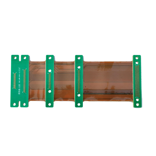
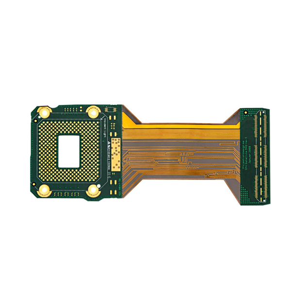
Rigid Flex PCBs

Rigid Flex PCBs seamlessly integrate the advantages of rigid and flexible circuit boards.This unique circuit board design not only inherits the high stability and load-bearing capacity of rigid boards, but also has the characteristics of space saving, bendable folding, and high connection density of flexible boards.
The manufacturing of Rigid Flex PCBs is a highly complex,in the manufacturing process, rigid areas typically use glass fiber reinforced epoxy resin substrates (such as FR-4), while flexible areas use film materials such as polyimide or polyester.
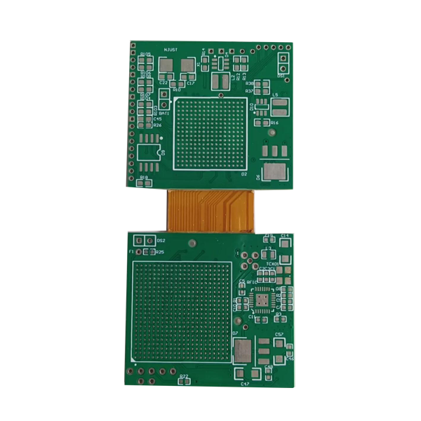
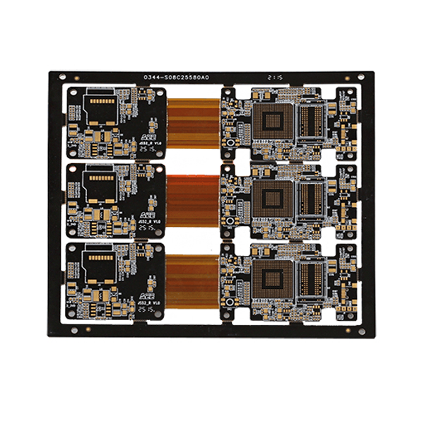
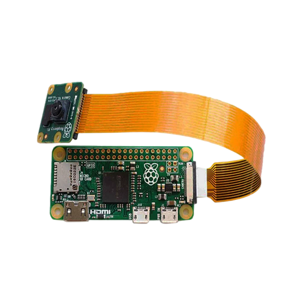
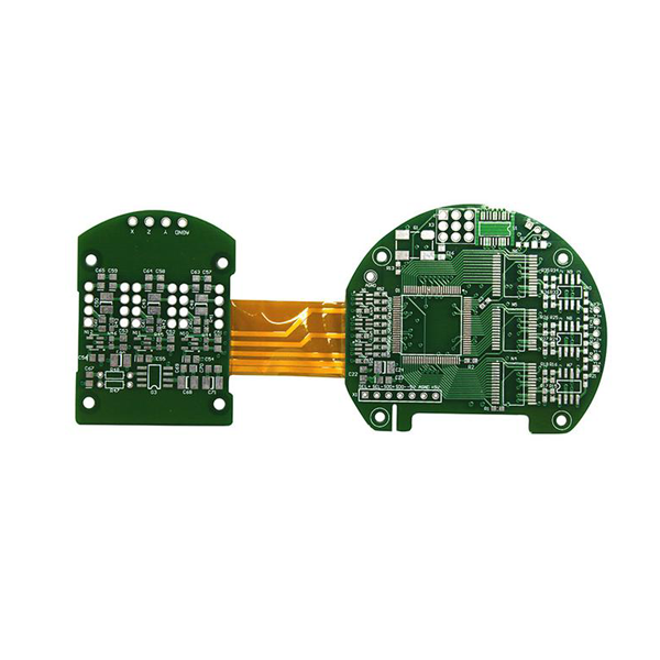
Product Showcase
Capabilities
| Capability | Parameter |
|---|---|
| Layer | 26L |
| 26L | 0.065 mm/0.065 mm |
| Min Hole/Pa Size | 0.10/0.35 mm |
| Rigid-Flex Thickness | 0.25-6.0mm |
| Drilling Accuracy | +/-0.05 mm |
| PTH Diameter Tolerance | +/-0.05 mm |
| Max Wpnl Size | 620 mm x 500 mm |
| Finish Copper (Flex Part) | 0.5-2oz |
| Finish Copper (Rigid Part) | 1-4oz |
| Surface Treatment |
ENIG Electric Gold IM-Ag Electric Ag HASL HASL-LF IM-Sn Electric Sn OSP Caborn Pt NI-Pd-AU |
| Max Board Thickness: PTH Diameter | 13:01 |
| Build Time | 7-20 Days |
Are you looking for a high-quality and full-range PCB fabrication, PCB assembly?
FAQ
Rigid Flex PCBs are printed circuit boards that combine the characteristics of both rigid and flexible circuit boards.
Their main advantage lies in providing higher design flexibility, allowing for complex interconnections to be achieved in a compact space while maintaining the stability of rigid regions and the bending ability of flexible regions.
This helps to reduce the overall device size, improve reliability, and lower costs.
The manufacturing process of Rigid Flex PCBs involves multiple key steps, including material selection, design layout, laser drilling, electroplating, etching, lamination, folding and assembly of flexible areas, etc.
Among them, the lamination step is particularly crucial because it requires precise bonding of rigid and flexible layers together while ensuring the reliability of interlayer connections.
In addition, the folding of flexible areas also requires precise control to avoid cracking or damage during the bending process.
When designing Rigid Flex PCBs, multiple factors need to be considered, including the overall size of the circuit board, layout of rigid and flexible areas, signal integrity, thermal management, material selection, and stacking structure.
Designers need to carefully plan signal paths to ensure efficient transmission of signals between rigid and flexible areas.
Meanwhile, it is also necessary to consider the matching of coefficient of thermal expansion (CTE) to avoid excessive stress during temperature changes.
Rigid Flex PCBs are widely used in various fields, including smartphones, tablets, wearable devices, medical equipment, aerospace systems, and automotive electronics.
They are particularly suitable for application scenarios that require high integration, compact design, and complex interconnection.
In these fields, Rigid Flex PCBs can provide excellent performance and reliability while meeting the demand for miniaturization and lightweighting.
To ensure the quality and reliability of Rigid Flex PCBs, a series of measures need to be taken.
Firstly, manufacturers need to select high-quality raw materials and ensure that every step of the manufacturing process meets strict process standards.
Secondly, strict testing and inspection are required, including electrical performance testing, reliability testing, and environmental adaptability testing.
In addition, designers also need to consider redundancy and fault tolerance mechanisms in their designs to improve the overall reliability and stability of the circuit board.
Through these measures, it can be ensured that Rigid Flex PCBs perform well in their final application, meeting the needs and expectations of customers.