HDI PCBs

HDI PCBs use micro blind hole/buried blind hole technology to achieve interconnection between different copper layers inside.Compared to traditional through-hole connections, HDI PCBs can achieve higher processing speeds and more functions, while reducing the surface area and thickness of circuit boards, making electronic devices more beautiful and compact.
HDI PCBs have a wide range of applications in fields such as data communication, automotive, and consumer electronics, especially in miniaturized electronic devices such as smartphones, tablets, and wearable devices.
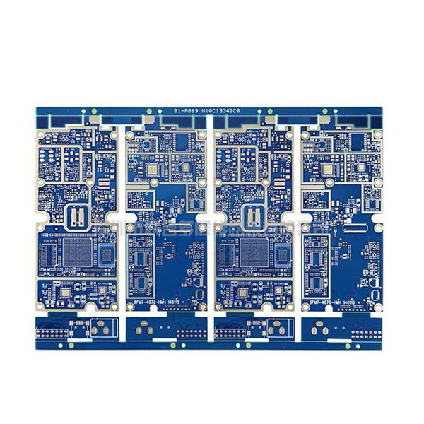
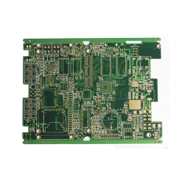
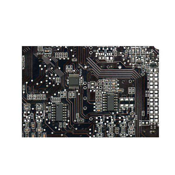
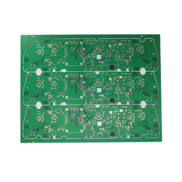
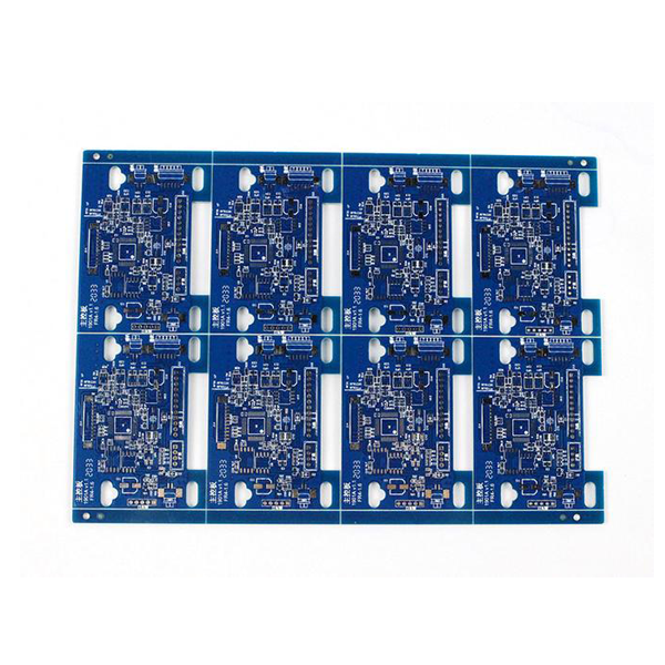
Product Showcase

Capabilities
| Capability | Parameter |
|---|---|
| Min. Line Width/Space | 2.5/2.5 |
| Max. Layer Count | 20 |
| Min. CCL Thickness | 50um |
| Min. Build-Up Thickness | 35um |
| Min. Microvia Design | 100um/200um |
| Min. Finished PTH Size | 0.15mm |
| Impedance Control | Impedance Tolerance:+/-5om or +/-10% |
| RoHs Certification | RoHs Certification |
| Lead Free Compliance | Available |
| Green Material-H/F | Available |
| Copper filled Microvia | Available |
| ELIC Level | 18 Layers |
Are you looking for a high-quality and full-range PCB fabrication, PCB assembly?
FAQ
High density interconnect printed circuit board is a circuit board that uses micro blind hole/buried blind hole technology to achieve high-density interconnect between different copper layers inside.
Compared with traditional PCBs, HDI PCBs have higher wiring density and smaller volume, which can meet the demand for electronic products to develop towards lightweight and high-performance.
In addition, HDI PCBs also exhibit superior performance in signal transmission speed, electrical performance, and reliability.
The manufacturing process of HDI PCBs involves multiple key technologies, among which laser drilling technology, electroplating filling technology, and lamination technology are the most critical.
HDI PCBs are widely used in various fields, especially in miniaturized electronic devices such as smartphones, tablets, and wearable devices.
In addition, with the increasing demand for high-performance and high reliability circuit boards in fields such as automotive electronics, medical electronics, and aerospace
HDI PCBs achieve high-density interconnection between different copper layers inside by using micro blind hole/buried blind hole technology and stacking technology.
Micro blind hole/buried blind hole technology enables wiring to be carried out in a smaller space, thereby increasing wiring density.
At the same time, multi-layer technology stacks multiple thin circuit boards together through multiple lamination and drilling processes, further increasing the number of wiring layers and the installation space for electronic components, thereby improving the overall wiring density.
HDI PCBs have multiple special requirements in the design and manufacturing process.
Firstly, due to the high wiring density of HDI PCBs, advanced EDA software is required for precise wiring during design.
Secondly, it is necessary to strictly control various process parameters during the manufacturing process, such as the aperture size of laser drilling and the filling quality of electroplating holes, to ensure the quality and performance of the product.
In addition, HDI PCBs also have special requirements for testing and inspection, requiring high-precision testing equipment and methods for electrical performance testing, reliability testing, etc.