BGA soldering is a process of packaging chips in a spherical matrix and connecting them to solder pads on a circuit board through solder balls. BGA soldering is a technically demanding and operationally complex process that requires strict adherence to process specifications and operating guidelines to ensure soldering quality and reliability of electronic products. The following are the main steps of BGA soldering:
Preparation work
Ensure a clean working environment: BGA soldering needs to be carried out in a clean, dust-free, and constant temperature environment.
Prepare welding materials: including BGA chips, solder paste, mounting adhesive, etc. At the same time, ensure that the solder balls are intact and the chip is not damaged.
Prepare welding equipment: Welding equipment includes welding furnace, hot air gun, microscope, solder paste printing machine, cleaning solution, X-ray detection equipment, etc.
PCB board processing
Cleaning PCB board: Use alcohol or specialized cleaning agents to clean the surface of the PCB board, removing oil and dust.
Dot mounting adhesive: Pre apply an appropriate amount of mounting adhesive to the BGA solder pads on the PCB board to secure the BGA chip.
Chip mounting and curing
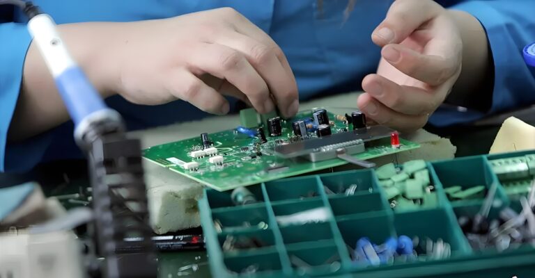
Placing BGA chips: Use a microscope and tweezers to accurately place the BGA chips on the solder pads on the PCB board.
Curing and mounting adhesive: Place the mounted PCB board in an oven and cure it according to the curing temperature and time of the mounting adhesive.
Solder paste printing and soldering
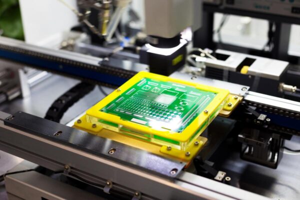
Printing solder paste: Select the appropriate solder paste, and use a solder paste printing machine to accurately print the solder paste on the BGA pads according to the size of the solder balls on the BGA chip and the requirements of the PCB board.
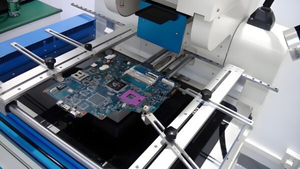
Set welding parameters: Select a suitable welding furnace based on the type of BGA chip and the material of the PCB board, and set the temperature curve of the welding furnace.
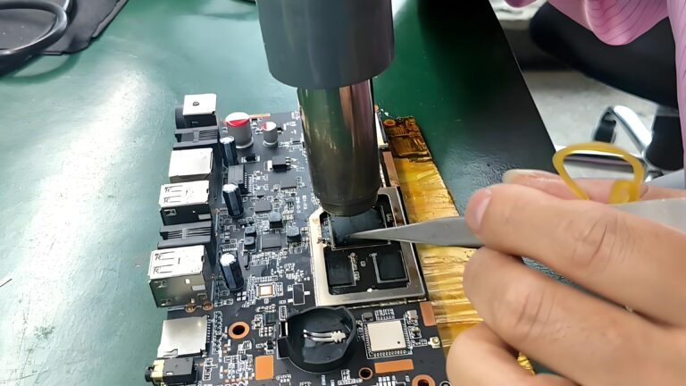
Welding: Place the assembled PCB board into a welding furnace and weld it according to the set temperature curve.
Post welding treatment and inspection
Cooling: Wait for the BGA chip to cool down before proceeding with subsequent operations.
Cleaning: Use cleaning solution to clean the PCB board after soldering, removing residual flux and solder slag.
Check welding quality: Use a microscope to inspect the welding quality, ensuring good welding between the solder ball and the solder pad, without virtual welding or short circuit. At the same time, X-ray inspection equipment is used to check the soldering quality of BGA chips to ensure the integrity and reliability of the soldering.
Handling of poor welding
Determine poor welding: Determine whether the welding is poor through visual inspection, functional testing, and other methods.
Dealing with poor welding: Corresponding measures need to be taken for poor welding.
By following the above steps, the BGA soldering process can be completed. It should be noted that BGA soldering is a technically demanding and operationally complex process that requires strict adherence to process specifications and operating guidelines to ensure soldering quality and reliability of electronic products.