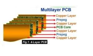
Multi-layer PCB design recommendations and examples (4, 6, 8, 10, and 12-layer boards) illustrate PCB design requirements.
1. The first layer is the complete grounding layer (shield);
2. There are no adjacent parallel wiring layers;
3. All signal layers are as close as possible to the grounding layer;
4. Critical signals are adjacent to the grounding layer and do not cross the partition.
Solution 1: There is a grounding layer below the component layer, and critical signals are assigned preferentially to the TOP layer. For layer thickness settings, the following suggestions can be used:
1. Meet impedance control;
2. The core board (GND to POWER) should not be too thick to reduce the distributed impedance of the ground plane; ensure the decoupling effect of the power plane.
Solution 2:
Defect: 1. The distance between power and ground is too far and the impedance of the power plane is too high.
2. The power and ground planes are very incomplete due to component pads, etc.
3. Signal impedance discontinuity due to incomplete reference plane.
Solution 3: Similar to solution 1 for cases where the master device is placed at the bottom or where critical signals are routed to the bottom.
6-layer PCB
Solution 3: Reduce the signal layers and add internal electrical layers. Despite the reduction in the number of layers available for routing, this PCB design solution addresses the common pitfalls of solutions 1 and 2.
Benefits:
Tightly coupled power and ground layers.
Each signal layer is directly adjacent to the internal electrical layer and has effective isolation from the other signal layers, so crosstalk is difficult to occur.
Signal layer 2 (inner_2) is adjacent to two internal electrical layers, GND (inner_1) and power (inner_3), which can be used to transmit high-speed signals. The two internal electrical layers effectively shield the signal layer_2 (inner layer_2) layer from external interference.
Solution 1: Use 4 signal layers and 2 internal power/ground layers with additional signal layers, which facilitates the wiring work between them.
Flaws: 1. Power and ground layers are too far apart and not sufficiently coupled.
2. Signal layer_2 (inner_layer_2) and signal layer_3 (inner_layer_3) are directly adjacent to each other, with poor signal isolation and easy crosstalk.
8-layer PCB
10-layer PCB
12-layer PCB
Personal summary:
1. The critical signal layer of the PCB design should be adjacent to ground and GND should be adjacent to the power supply to reduce power plane impedance.
2. Do not be adjacent to the signal layer to increase the isolation between signals and avoid crosstalk.
3. The signal layer should be as close to the grounding layer as possible. Do not run parallel wiring between adjacent layers.
4. For transmission lines, the top and bottom layers are analyzed using the microstrip line model, and the internal signal layers are analyzed using the ribbon line model. The signal layers on both sides of the baseboard are 6 layers/ 10 layers and 14 layers 18 layers, preferably using software.
5. If other power sources are available, it is best to run thick wires on the signal layer and try not to separate the electrical grounding layers. High speed lines are best into the inner layer. The top and bottom layers are susceptible to outside temperature, humidity and air, and are not easily stabilized.

