Flexible PCBs
Flexible PCBs are circuit boards made from flexible substrates such as polyimide film, polyamide film, etc. The main materials include conductive materials, insulating materials, and substrates.The conductive material is usually copper foil, which forms a circuit pattern after rolling or etching.Insulating materials are used to isolate conductive layers and prevent short circuits.
The manufacturing process of Flexible PCBs includes multiple steps such as cutting and drilling circuit boards, creating circuit graphics, laying conductive layers, and soldering.
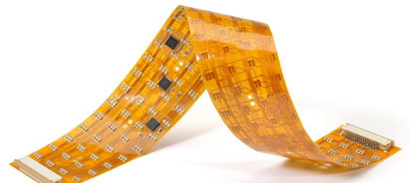
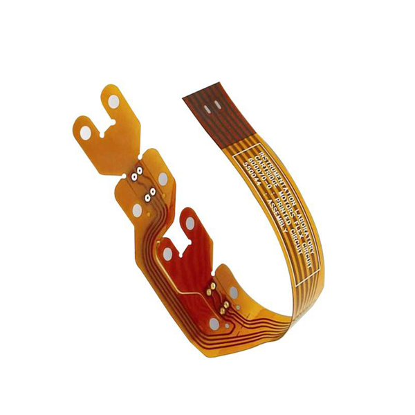
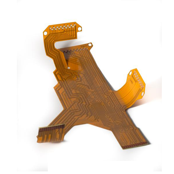
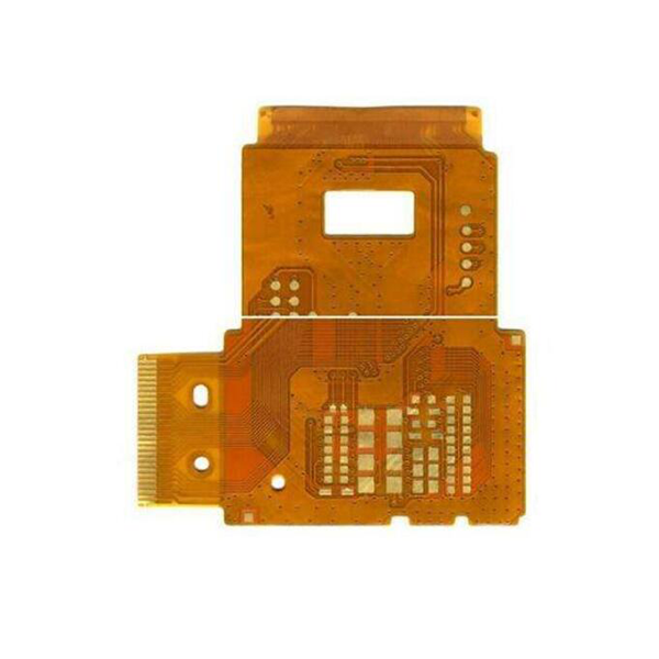
Product Showcase


Capabilities
| Capability | Parameter |
|---|---|
| PCB Type | Flexible PCB |
| Quality Grade | Standard IPC 2 |
| Material |
PI PET |
| Number of Layers |
1 Layer 2 Layers 4 Layers 6 Layers 8 Layers |
| Max PCB Size | 1 Layer: 4000mm x 240mm 2 Layers: 800mm x 240mm Multi-layers: 350mm x 240mm |
| Board Size Tolerance (Outline) | ±0.1mm |
| Soldering Pad Diameter | ≥0.3mm |
| Quality Grade | Standard IPC 2 |
| Lead Time | 5-7 Days |
| Coverlay | Yellow, White, Black, None |
| Coverlay Opening Size | ≥0.6mm x 0.6mm |
| Min Spacing Colverlay to Soldering Pad | ≥0.15mm |
| Soldermask Color | Green and Others |
| Soldermask Bridge |
Green: ≥0.1mm Others: ≥0.15mm |
| Minimum Character Width (Legend) | ≥0.7mm |
| Minimum Character Height (Legend) | ≥0.8mm |
| Min Spacing from Silkscreen to Soldering | ≥0.2mm |
| Surface Finish |
ENIG OSP Immersion Tin Chemical Silver |
| Impedance Control |
Single-ended 50Ω Differential Pairs100Ω Tolerance ±10% |
| Stiffener Material |
PI FR-4 Aluminum Steel |
| Edge Rail Width | ≥10mm |
Are you looking for a high-quality and full-range PCB fabrication, PCB assembly?
FAQ
The main substrate of flexible circuit boards is usually polyester film or polyimide film.
These materials have good flexibility and high temperature resistance, which can meet the needs of flexible circuit boards in dynamic applications such as bending and folding.
A layer of conductive material, usually copper foil, is deposited on the substrate of a flexible circuit board through a specific process.
The thickness of the conductive layer can be adjusted as needed to meet the requirements of different application scenarios for current transmission capacity and mechanical strength.
Substrate preparation: Select and prepare substrates such as polyester film or polyimide film that meet the requirements.
Preparation of conductive layer: Plating copper foil or other conductive materials on the substrate.
Circuit pattern formation: Excess copper foil on the conductive layer is removed through processes such as photo painting and etching to form the desired circuit pattern.
Process processing: After the formation of the circuit pattern, coating protective layer, curing, hole drilling, electroplating and other processes are carried out to increase the protection performance and reliability of the circuit board.
Finished product inspection: Conduct strict finished product inspection on flexible circuit boards, including appearance inspection, circuit connectivity testing, pad reliability testing, and other multiple tests to ensure that the circuit board meets quality requirements.
Before sampling, the design of flexible circuit boards needs to undergo strict review.
This process mainly checks the rationality, feasibility, and potential manufacturing issues of the design.
Design review is usually completed by a professional team of engineers who will carefully evaluate the design documents based on experience and technical specifications to ensure the quality and reliability of the final product.