High Frequency PCBs

High frequency printed circuit board is a type of circuit board designed specifically to meet the requirements of high-frequency signal transmission.
Generally speaking, high frequency can be defined as a frequency above 1GHz.Its various physical properties, accuracy, and technical parameters require very high standards, and it is commonly used in fields such as automotive collision prevention systems, satellite systems, and radio systems.
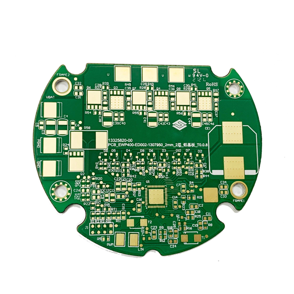
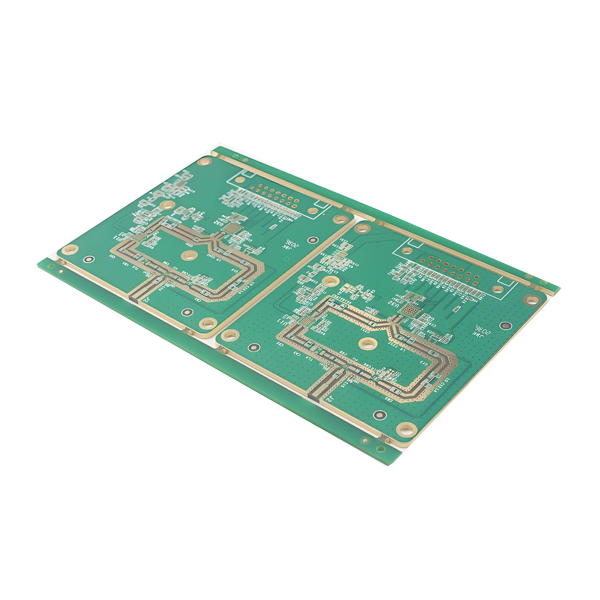
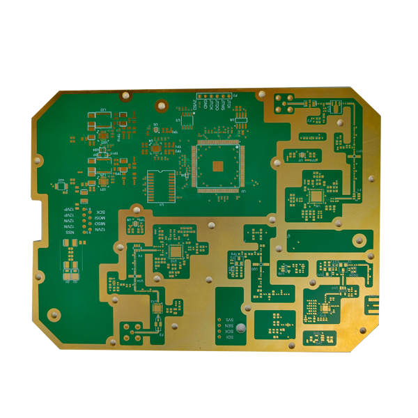
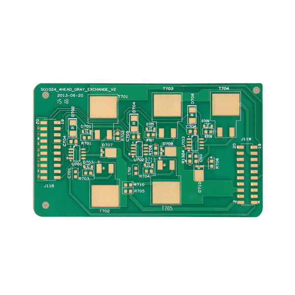
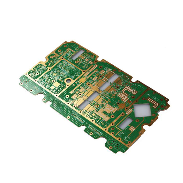
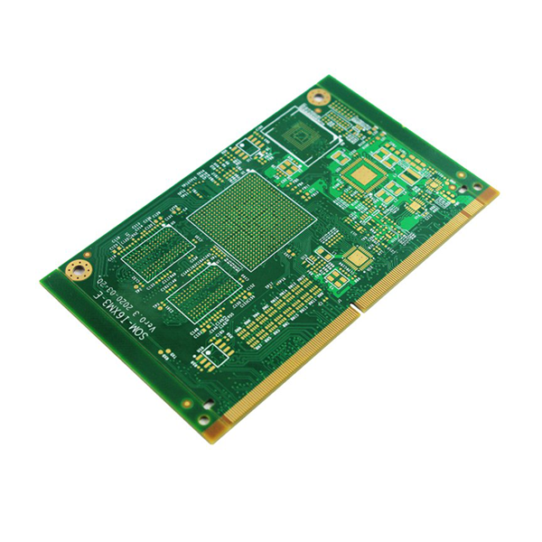
Product Showcase
Capabilities
| Capability | Parameter |
|---|---|
| Material | RO4003C, RO4350B, RO3003, RO3010, RT5880 |
| Min Track/Spacing | 3/3mil |
| Min Hole Size | 0.15mm |
| Finished Cooper | 1-2oz |
| Board Thickness | 0.2-3.2mm |
| Surface Finishing | Immersion Gold, OSP, Hard Gold,Immersion SIlver,Enepig |
| Finsih Cooper | 0.5-13oz |
| Solder Mask | Green, Red, Yellow, Blue, White, Black, Purple, Matte Black, Matte Green |
| Silkscreen | White, Black |
| Via Process |
Tenting Vias Plugged Vias Vias not covered |
| Tenting |
Fly Probe Testing AOI Testing |
| Build time | 7-10 Days |
| Lead Time | 2-3 Days |
Are you looking for a high-quality and full-range PCB fabrication, PCB assembly?
FAQ
High Frequency PCBs,
High frequency printed circuit board is a type of circuit board designed specifically to meet the requirements of high-frequency signal transmission.
They use special substrates and manufacturing processes to ensure excellent electrical performance and stability at high frequencies.
This type of circuit board has a wide range of applications in wireless communication, radar systems, satellite communication, high-speed data transmission, and other fields.
The manufacturing process of High Frequency PCBs involves multiple key steps, including:
Substrate selection and pretreatment: Select suitable substrates and perform pretreatment steps such as cleaning and drying.
Circuit fabrication: Creating circuit patterns on substrates through processes such as photolithography and etching.
Hole processing: Laser drilling or mechanical drilling technology is used to create micro holes for interlayer connection.
Electroplating and filling: Electroplating treatment of holes to form conductive channels, and filling of blind or buried holes.
Layering and curing: Multi layer circuit boards are pressed together and the adhesion between layers is enhanced through a high-temperature curing process.
Surface treatment: Coating, gold plating, tin spraying and other treatments are applied to the surface of the circuit board to improve its reliability and solderability.
Testing and Inspection: Conduct rigorous electrical performance testing, reliability testing, and visual inspection to ensure product quality.
High Frequency PCBs require special substrates mainly because these substrates have low dielectric constant (Dk) and low loss tangent angle (Df).
These two parameters have a direct impact on the transmission performance of high-frequency signals:
Low dielectric constant: The dielectric constant determines the propagation speed of signals in materials.
The lower the dielectric constant, the faster the signal propagation speed and the smaller the delay, which is crucial for high-speed data transmission.
Low loss tangent angle: The loss tangent angle reflects the degree to which a material absorbs signal energy at high frequencies.
The smaller the tangent angle of the loss, the smaller the signal attenuation, and the higher the transmission efficiency.
In the design of High Frequency PCBs, impedance matching is a key step in ensuring lossless signal transmission, reducing reflection, and improving signal quality.
To achieve impedance matching, the following measures need to be taken:
Control line width and spacing: By adjusting the width and spacing of the wires on the PCB, as well as the thickness of the dielectric layer, the characteristic impedance can be precisely controlled to match the load impedance.
Using impedance control stacking: Reasonably arranging the position of the power layer, geological layer, and dielectric material can optimize the impedance characteristics of the entire board.
Terminal matching: Adding matching components (such as resistors, ferrite beads, etc.) at the end of the signal line can absorb reflected waves and reduce signal reflection.
Differential Pair Design: For high-speed differential signals, by maintaining strict symmetry in parameters such as length, line width, and spacing between two signal lines, a good impedance matching can be naturally formed.
Quality control is crucial in the manufacturing process of High Frequency PCBs.
To ensure product quality, the following measures need to be taken:
Strict screening of materials: Select substrates and auxiliary materials that meet the requirements to ensure the electrical performance and thermal stability of the materials.
Optimize manufacturing process: Strictly control parameters such as temperature, pressure, and time during the manufacturing process to ensure the accuracy and consistency of each step.
Strengthen testing and inspection: Conduct strict electrical performance testing, reliability testing, and visual inspection to promptly identify and address potential quality issues.
Continuous improvement and feedback: Based on test results and customer feedback, continuously optimize manufacturing processes and quality control procedures.